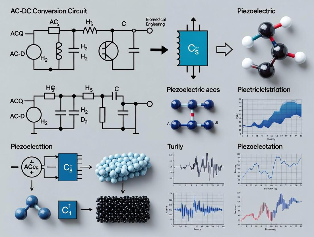
Powering Biomedical Devices: Advanced AC-DC Conversion Circuits for Piezoelectric Energy Harvesting
This article provides a comprehensive technical guide on AC-DC conversion circuits tailored for piezoelectric transducers in biomedical applications.
Powering Biomedical Devices: Advanced AC-DC Conversion Circuits for Piezoelectric Energy Harvesting
Abstract
This article provides a comprehensive technical guide on AC-DC conversion circuits tailored for piezoelectric transducers in biomedical applications. Aimed at researchers and drug development professionals, it explores the foundational principles of piezoelectricity and rectification, details methodologies for full-wave and voltage-doubler circuits, offers troubleshooting for impedance mismatching and low-voltage startup, and presents validation metrics and comparisons of recent circuit architectures. The content synthesizes current research to enable the development of efficient, self-powered implantable sensors and biomedical systems.
From Vibration to Voltage: Core Principles of Piezoelectric Harvesting and Rectification
Application Notes: Energy Harvesting from Physiological Motion
Piezoelectric materials convert mechanical strain from physiological motions into alternating current (AC) electrical signals. This principle enables the development of self-powered medical devices and biosensors. The following table summarizes key performance metrics from recent studies.
Table 1: Quantitative Performance of Selected Piezoelectric Energy Harvesters for Physiological Motion
| Piezoelectric Material/Structure | Implantation Site / Motion Source | Open-Circuit Voltage (Vpp AC) | Output Power Density | Frequency of Motion (Hz) | Reference Year |
|---|---|---|---|---|---|
| PZT thin film on flexible substrate | Diaphragm (Respiratory) | 2.1 | 0.18 µW/cm² | 0.2 - 0.33 | 2023 |
| PVDF-TrFE nanofiber mat | Cardiac Apex (Heartbeat) | 4.8 | 1.2 µW/cm³ | 1.0 - 1.7 | 2024 |
| Biodegradable ZnO thin film | Peripheral Muscle (Limb Movement) | 0.85 | 8.6 nW/cm² | 0.5 - 3.0 | 2023 |
| Lead-free KNN-based composite | Jaw (Chewing) | 6.5 | 3.4 µW/cm² | 1.0 - 2.5 | 2024 |
| PZT ribbon with serpentine design | Lung Surface (Breathing) | 3.2 | 0.42 µW/cm² | 0.17 - 0.25 | 2023 |
Key Applications:
- Implantable Biosensors: Harvesting energy for continuous glucose monitors, neural activity sensors, and intracranial pressure monitors.
- Drug Delivery Systems: Powering miniaturized, programmable micropumps for chronotherapeutic drug release.
- Leadless Pacemakers: Supplementing battery life by converting cardiac motion into electrical energy.
- Wearable Health Monitors: Powering flexible patches that monitor vital signs (e.g., respiration rate, pulse).
Experimental Protocol: In-Vitro Characterization of a Piezoelectric Harvester for Muscle Motion
This protocol details the methodology for evaluating a flexible piezoelectric device intended for implantation on skeletal muscle.
AIM: To characterize the AC electrical output of a polyvinylidene fluoride-trifluoroethylene (PVDF-TrFE) based harvester under simulated physiological strain conditions.
MATERIALS:
- Fabricated PVDF-TrFE harvester (5 mm x 20 mm, encapsulated in biocompatible silicone).
- Electro-mechanical tester (e.g., Bose ElectroForce or similar with calibrated load cell).
- High-input impedance data acquisition system (DAQ, >10 MΩ) with differential probes.
- Oscilloscope.
- Custom mounting fixtures compatible with the tester and the harvester.
- Phosphate-buffered saline (PBS) solution, pH 7.4, at 37°C.
- Environmental chamber for the mechanical tester.
PROCEDURE:
- Mounting: Secure the ends of the piezoelectric harvester onto the fixtures of the electro-mechanical tester, ensuring the active bending zone is free. Connect the device's electrodes to the DAQ system.
- Environmental Conditioning: Place the mounted setup into the environmental chamber. Submerge the harvester in PBS solution at 37°C. Allow temperature to equilibrate for 30 minutes.
- Mechanical Stimulation Programming: Program the mechanical tester to apply cyclic tensile strain.
- Waveform: Sinusoidal.
- Strain Amplitude: Ramp from 0.1% to 1.5% in increments.
- Frequency Sweep: At each strain amplitude, perform a frequency sweep from 0.5 Hz to 5 Hz, covering the range of skeletal muscle motion.
- Cycles: 50 cycles per parameter set to ensure stable output.
- Data Acquisition: Simultaneously record the applied strain (from tester) and the generated AC voltage (from DAQ) for all test cycles. Use the oscilloscope to visually confirm waveform integrity.
- Load Characterization: At optimal strain/frequency (e.g., 1.0% strain, 2 Hz), connect a variable resistor load across the harvester terminals. Measure the RMS voltage across the load while varying resistance from 1 kΩ to 100 MΩ. Calculate output power (P = V²/R).
DATA ANALYSIS:
- Plot Open-Circuit Voltage (peak-to-peak) vs. Strain Amplitude and Frequency.
- Plot Output Power vs. Load Resistance to determine the optimal load and maximum power transfer.
- Calculate the effective piezoelectric coefficient (d₃₁ or d₃₃) from the slope of the charge-strain relationship.
The Scientist's Toolkit: Research Reagent Solutions
Table 2: Essential Materials for Piezoelectric Biomaterial Development & Testing
| Item / Reagent | Function / Purpose |
|---|---|
| Poly(vinylidene fluoride-co-trifluoroethylene) (PVDF-TrFE) | A flexible, biocompatible, and chemically inert piezoelectric polymer, often solution-processed into films or electrospun into fibers for soft, conformal harvesters. |
| Polydimethylsiloxane (PDMS), medical grade | A silicone elastomer used as a flexible, biocompatible encapsulation layer to protect the piezoelectric element from the biofluid environment and insulate electrical contacts. |
| Phosphate-Buffered Saline (PBS), pH 7.4 | A standard isotonic solution used for in-vitro testing to simulate the ionic composition and osmotic pressure of physiological fluids. |
| Piezoresponse Force Microscopy (PFM) Kit | A set of conductive cantilever tips and calibration standards used with an atomic force microscope (AFM) to locally map and quantify piezoelectric response at the nanoscale. |
| Biocompatible Epoxy (e.g., EP42HT-2Med) | Used for securing electrical connections and component assembly in implantable prototypes, offering long-term stability in wet environments. |
| Flexible Conductive Ink (e.g., Ag/AgCl flake in silicone) | Creates stretchable, low-impedance electrodes on flexible piezoelectric substrates that can withstand repeated deformation without cracking. |
| Impedance Analyzer (e.g., Keysight E4990A) | Characterizes the complex electrical impedance of the piezoelectric device across a frequency range, critical for designing matching AC-DC conversion circuits. |
Visualizations
Diagram Title: Workflow from Body Motion to Powered Device
Diagram Title: Piezoelectric Biomedical Harvester Development Protocol
Application Notes: The Fundamental Necessity of Rectification
In the context of research on AC-DC conversion circuits for piezoelectric transducers, the rectification stage is an absolute prerequisite for practical energy harvesting and utilization. Piezoelectric materials generate alternating current (AC) in response to mechanical vibrations—a ubiquitous but irregular energy source in environments from industrial machinery to biomedical implants. To power consistent, usable direct current (DC) for sensors, microcontrollers, or drug delivery systems, this AC must be converted. Rectification, the process of converting bidirectional AC to unidirectional current, is the critical first step in this power conditioning chain. Without it, the harvested energy cannot be stored in capacitors or batteries, nor can it reliably power the vast majority of semiconductor-based electronic components and integrated circuits, which require stable DC bias voltages to operate. This conversion enables the transition from laboratory transduction principles to autonomous, self-powered devices for long-term monitoring and actuation.
Quantitative Comparison of Rectifier Topologies for Piezoelectric Harvesting
The choice of rectifier architecture significantly impacts the efficiency of energy extraction from a piezoelectric source. Key performance metrics include the input voltage threshold for activation and power conversion efficiency (PCE). The following table summarizes data from recent experimental studies on low-power (< 10 mW) piezoelectric energy harvesting.
Table 1: Performance Metrics of Common Rectifier Circuits for Piezoelectric Transducers
| Rectifier Topology | Typical Operating Voltage Range | Approximate Power Conversion Efficiency (PCE) | Key Advantage | Primary Limitation |
|---|---|---|---|---|
| Full-Wave Bridge (Passive) | > 0.7V (Diode Vf dependent) | 40-70% | Simplicity, robustness | High threshold voltage loss |
| Voltage Doubler (Cockcroft-Walton) | Very Low (< 0.3V) | 50-75% | Effective at low voltages | Requires more capacitors, load-dependent |
| Active Diode (Synchronous) | < 0.1V (MOSFET Rds(on) dependent) | 70-90% | Very low forward voltage drop | Requires control circuitry, complexity |
| Switching Boost Rectifier | Very Low (< 0.1V) | 65-85% | Integrated voltage step-up, high efficiency | Highest complexity, control overhead |
Experimental Protocol: Characterizing a Piezoelectric Energy Harvester with Full-Wave Bridge Rectification
Objective: To measure the DC output power and efficiency of a piezoelectric transducer (PZT) coupled with a passive full-wave bridge rectifier under controlled mechanical excitation.
Materials & Reagents:
- Piezoelectric cantilever (e.g., Mide Technology V21BL or equivalent).
- Electrodynamic shaker with power amplifier.
- Function generator.
- Full-wave bridge rectifier (composed of 4 Schottky diodes, e.g., BAT54S).
- Storage capacitor (e.g., 10 µF to 100 µF electrolytic).
- Programmable electronic load or precision resistor decade box.
- Oscilloscope with high-impedance probes.
- Laser displacement sensor (or calibrated accelerometer).
- Data acquisition system.
Procedure:
- Setup Calibration: Mount the PZT cantilever securely to the shaker armature. Use the laser displacement sensor to measure the tip displacement of the cantilever. Drive the shaker via the function generator and power amplifier at the PZT's resonant frequency (determined via a prior frequency sweep). Calibrate the input acceleration (g-level) to the shaker's driving voltage.
- Circuit Assembly: Solder the full-wave bridge rectifier using the Schottky diodes. Connect the output of the PZT to the AC input terminals of the bridge. Connect the positive and negative DC output terminals of the bridge to the storage capacitor in parallel with the programmable electronic load.
- Open-Circuit Voltage Measurement: Set the electronic load to a high-resistance state (>1 MΩ). Subject the PZT to a fixed mechanical excitation (e.g., 0.5g at resonance). Use the oscilloscope to measure the peak-to-peak open-circuit AC voltage (VAC(p-p)) directly from the PZT terminals. Then, measure the steady-state DC voltage (VDC(oc)) across the storage capacitor.
- Power Delivery Measurement: Set the electronic load to a specific resistive value (RL). Allow the system to reach steady-state. Record the DC voltage (VDC) across the load. Calculate the delivered DC power: PDC = VDC2 / RL.
- Efficiency Calculation: For the same excitation condition, measure the AC voltage (VAC(rms)) and current (IAC(rms)) at the input to the rectifier using oscilloscope math functions. Calculate the available AC input power: PAC = VAC(rms) * IAC(rms). The rectifier stage efficiency is: ηrect = (PDC / PAC) * 100%.
- Sweep Parameters: Repeat steps 4-5 for a range of load resistances (e.g., 1 kΩ to 1 MΩ) and/or input acceleration levels. Plot PDC vs. RL to identify the optimal load for maximum power transfer.
The Scientist's Toolkit: Research Reagent Solutions for Piezoelectric Energy Harvester Testing
Table 2: Essential Materials for Piezoelectric AC-DC Conversion Research
| Item | Function/Explanation |
|---|---|
| Lead Zirconate Titanate (PZT) Cantilevers | Standard piezoelectric element providing high electromechanical coupling; the AC voltage source for the experiment. |
| Low-Dropout Schottky Diodes (e.g., BAT54 series) | Core rectification component; minimizes the forward voltage loss (~0.3V) compared to standard silicon diodes (~0.7V), crucial for low-voltage PZT outputs. |
| Polymer-based Solid-State Capacitors | Energy storage buffer; low equivalent series resistance (ESR) is critical for efficiently capturing short, high-frequency current pulses from the rectifier. |
| Wideband Electrodynamic Shaker System | Provides precise, controllable, and repeatable mechanical excitation to the PZT at specified frequencies and amplitudes. |
| Precision Programmable DC Electronic Load | Enables systematic sweeps of load resistance to find the maximum power point (MPP) of the complete harvesting circuit without manual resistor swapping. |
Visualization: Piezoelectric Harvesting System Workflow
Diagram Title: Piezoelectric Energy Harvesting Signal Chain
Visualization: Rectifier Topology Decision Logic
Diagram Title: Rectifier Selection Logic Flow
This application note details the core electrical characteristics of piezoelectric transducers (PZTs) essential for their integration into AC-DC conversion circuits. As part of a broader thesis on energy harvesting for biomedical applications—such as powering implantable drug delivery systems—understanding these parameters is fundamental. Efficient AC-DC conversion maximizes harvested power from mechanical vibrations, directly impacting the viability of self-powered medical devices.
Core Electrical Characteristics
Fundamental Parameters & Data
Piezoelectric transducers are governed by a constitutive equation coupling mechanical and electrical domains. For power harvesting, the simplified equivalent circuit is a sinusoidal current source, (ip(t) = Ip \sin(\omega t)), in parallel with an internal capacitance ((Cp)) and resistance ((Rp)). Key measurables are derived from this model.
Table 1: Key Electrical Characteristics of Representative Piezoelectric Transducers
| Transducer Type/Material | Typical Open-Circuit Voltage (Voc), peak | Typical Short-Circuit Current (Isc), peak | Internal Capacitance, Cp (nF) | Optimal Resistive Load (kΩ) | Max Power Output (µW) |
|---|---|---|---|---|---|
| PZT-5A (Ceramic, 1 cm²) | 10 - 50 V | 10 - 50 µA | 20 - 100 | 50 - 500 | 100 - 1000 |
| PVDF (Polymer Film) | 5 - 20 V | 1 - 10 µA | 0.5 - 5 | 500 - 5000 | 5 - 50 |
| MFC (Macro Fiber Composite) | 30 - 100 V | 5 - 20 µA | 5 - 30 | 200 - 1000 | 200 - 500 |
| ZnO Nanowire Array | 0.1 - 2 V | 0.01 - 0.5 µA | 0.01 - 0.1 | 1000 - 10000 | 0.001 - 0.1 |
Note: Values are highly dependent on excitation frequency, amplitude, transducer geometry, and mounting. Data compiled from recent literature (2021-2024).
Characteristic Definitions
- Open-Circuit Voltage (Voc): The peak voltage measured across the transducer terminals when no load is connected. It represents the maximum potential difference the transducer can generate under specific mechanical excitation.
- Short-Circuit Current (Isc): The peak current measured when the transducer terminals are connected with negligible impedance. It represents the maximum charge displacement current.
- Optimal Load (Zopt): The load impedance (often purely resistive for initial analysis) at which the electrical power delivered to the load is maximized. For a resistive load ((RL)), (Z{opt} \approx 1/(\omega Cp)) at the excitation frequency (\omega), neglecting (Rp).
Experimental Protocols
Protocol 1: Measurement of Voc, Isc, and Cp
Objective: To characterize the basic electrical output parameters of a PZT. Materials: See Scientist's Toolkit. Method:
- Mounting: Securely mount the PZT to a calibrated shaker or vibration source using a recommended adhesive (e.g., cyanoacrylate).
- Excitation: Apply a known, fixed sinusoidal mechanical excitation (e.g., 1g RMS at 100 Hz). Record frequency ((f)) and acceleration ((a)).
- Voc Measurement: Connect a high-impedance oscilloscope or differential voltage probe (>10 MΩ) directly across the PZT leads. Measure the peak sinusoidal voltage. (V{oc} = V{measured, peak}).
- Isc Measurement: Replace the oscilloscope with a low-resistance current sense resistor (e.g., 10-100 Ω) or a current probe. Measure the peak voltage across the sense resistor and calculate (I{sc} = V{sense, peak} / R_{sense}).
- Cp Measurement: Disconnect the PZT from the shaker. Using an LCR meter, measure the capacitance between the PZT leads at a low frequency (e.g., 1 kHz). This is the internal capacitance (C_p).
Protocol 2: Determination of Optimal Resistive Load and Maximum Power
Objective: To experimentally find the load resistance that maximizes power output. Method:
- Set up the PZT under the same fixed mechanical excitation as in Protocol 1.
- Connect a variable decade resistor box or a set of precision resistors across the PZT terminals.
- For each load resistor value ((RL)), use an oscilloscope to simultaneously measure the peak voltage ((V{L,peak})) across the load and the peak current ((I_{L,peak})) through it.
- Calculate RMS power for each load: (P{L, RMS} = (V{L,peak} / \sqrt{2}) \times (I{L,peak} / \sqrt{2}) = (V{L,peak} \times I_{L,peak}) / 2).
- Plot (P{L, RMS}) versus (RL). The resistance at the peak of the curve is the optimal resistive load ((R_{opt})).
- The corresponding power is the maximum harvestable power for a simple resistive load.
Diagrams for Characterization & Circuit Integration
Title: PZT Characterization & Optimal Load Determination Workflow
Title: From Piezoelectric Effect to Key Electrical Parameters
The Scientist's Toolkit: Research Reagent Solutions & Essential Materials
Table 2: Essential Materials for PZT Electrical Characterization
| Item / Reagent | Function / Explanation |
|---|---|
| Piezoelectric Transducer | Device Under Test (DUT). Common types: PZT ceramics (high output), PVDF films (flexible), MFCs (robust). |
| Electrodynamic Shaker | Provides controlled, reproducible mechanical vibration excitation at known frequencies and amplitudes. |
| Function Generator & Amp | Drives the shaker with a clean sinusoidal signal. Allows precise control of excitation frequency. |
| Low-Noise Charge Amplifier | Alternative to voltage measurement; directly converts piezoelectric charge to voltage, minimizing cable effects. |
| High-Impedance Oscilloscope | Measures high-voltage signals without loading the PZT circuit (input impedance ≥10 MΩ). |
| Precision LCR Meter | Measures the internal capacitance (Cp) and dielectric loss of the PZT at rest. |
| Variable Decade Resistor Box | A set of high-precision, switchable resistors used to sweep load resistance (RL) during optimization. |
| Calibration Accelerometer | Mounted near the PZT to accurately measure the applied mechanical acceleration input. |
| Low-Capacitance Coaxial Cable | Minimizes signal attenuation and parasitic capacitance during high-impedance voltage measurements. |
| Anisotropic Conductive Adhesive | For mounting PZTs without shorting electrodes; maintains mechanical coupling. |
Within research into AC-DC conversion circuits for piezoelectric energy harvesting transducers, the standard diode bridge rectifier remains a fundamental interface component. Piezoelectric transducers generate low-voltage, alternating current (AC) output under mechanical excitation, necessitating efficient rectification for powering microelectronic devices or sensors. This application note details the operation, inherent efficiency limits, and critical threshold voltage challenges of the diode bridge rectifier in this specific research context, providing protocols for empirical characterization.
Operation Principle
A standard full-wave bridge rectifier employs four diodes arranged in a bridge configuration. It converts bidirectional AC input from a piezoelectric transducer into unidirectional pulsating DC output.
- Positive Half-Cycle: Current flows through one diode pair to the load.
- Negative Half-Cycle: Current flows through the other diode pair, maintaining the same polarity across the load.
The output is subsequently smoothed by a filter capacitor (C_f).
Quantitative Analysis of Efficiency Limits and Voltage Challenges
The primary efficiency limitation stems from the forward voltage drop (V_f) across each diode. For a standard silicon p-n junction diode, V_f is approximately 0.7V. During each half-cycle, the input AC voltage must overcome two series diode drops (2V_f ≈ 1.4V). For low-voltage piezoelectric outputs (often < 5V peak), this represents a significant loss, reducing the available output voltage and conversion efficiency.
Table 1: Impact of Diode Threshold on Rectifier Performance for Piezoelectric Inputs
| Piezoelectric Open-Circuit Voltage (V_peak) | Ideal DC Output (V) | Practical DC Output (considering 2*V_f loss) | Estimated Power Loss Percentage |
|---|---|---|---|
| 1.5 V | 1.5 V | ~0.1 V (severely clipped) | > 90% |
| 3.0 V | 3.0 V | ~1.6 V | ~ 44% |
| 5.0 V | 5.0 V | ~3.6 V | ~ 28% |
| 10.0 V | 10.0 V | ~8.6 V | ~ 14% |
Table 2: Comparison of Diode Technologies for Low-Voltage Rectification
| Diode Type | Typical Forward Voltage (V_f) | Advantage | Disadvantage |
|---|---|---|---|
| Standard Silicon (1N4007) | 0.65 - 1.00 V | Low cost, robust | High loss for low-voltage inputs |
| Schottky (e.g., 1N5817) | 0.15 - 0.45 V | Lower V_f, faster switching | Higher reverse leakage current, moderate cost |
| Germanium | ~0.3 V | Low turn-on voltage | Temperature sensitivity, less common |
| Active (Synchronous) | ~0.05 V (Rdson dependent) | Very low effective voltage drop, high efficiency | Complex drive circuitry, higher cost, parasitics |
Experimental Protocols
Protocol 4.1: Characterizing Rectifier Efficiency with Piezoelectric Input
Objective: To measure the voltage and power efficiency of a standard diode bridge under simulated piezoelectric excitation. Materials: Function generator, standard diode bridge (1N400x or equivalent), Schottky diode bridge (1N581x or equivalent), load resistors (10 kΩ to 1 MΩ), oscilloscope, digital multimeters (2), filter capacitor (e.g., 10 µF), solderless breadboard. Procedure:
- Set the function generator to produce a sinusoidal waveform with frequency 50-200 Hz (typical for many piezoelectric transducers) and variable amplitude (1-10 V_peak).
- Construct the standard diode bridge rectifier circuit with a filter capacitor and a load resistor (e.g., 100 kΩ) on the breadboard.
- Connect the function generator output to the AC input terminals of the bridge.
- Using Oscilloscope Channel 1, measure and record the peak input voltage (V_in_peak). Using Channel 2, measure the DC output voltage (V_out_dc) across the load.
- Use DMMs to precisely measure the RMS input voltage and DC output voltage. Calculate input power (P_in = V_in_rms² / R_source_est) and output power (P_out = V_out_dc² / R_load). Note: The source impedance must be estimated or measured separately.
- Calculate voltage efficiency: η_V = (V_out_dc / V_in_peak) * 100%.
- Calculate power efficiency: η_P = (P_out / P_in) * 100%.
- Repeat steps 4-7 for varying input voltages and load resistances.
- Replace the standard diode bridge with a Schottky diode bridge and repeat the entire experiment.
- Tabulate results for comparative analysis.
Protocol 4.2: Threshold Voltage Drop Measurement
Objective: To directly measure the forward voltage drop of the rectifier bridge as a function of current. Materials: DC power supply, current-limiting resistor (1 kΩ), diode bridge, ammeter, voltmeter. Procedure:
- Connect the DC power supply in series with the current-limiting resistor, the ammeter, and the DC output terminals of the bridge (treating it as a two-terminal device). Leave AC input terminals open.
- Connect the voltmeter directly across the DC output terminals.
- Slowly increase the supply voltage from 0V. The bridge will conduct when the voltage exceeds 2V_f.
- Record the voltage (V_bridge) and current (I) at multiple points as current increases (e.g., 0.1mA, 1mA, 10mA).
- Plot V_bridge vs. I. The y-intercept approximates the total threshold voltage (2V_f) of the bridge.
Diagrams and Visualizations
Title: Piezoelectric Energy Harvesting with Standard Diode Bridge
Title: Rectifier Selection Decision Flow
The Scientist's Toolkit: Research Reagent Solutions
Table 3: Essential Materials for Piezoelectric Rectifier Research
| Item / Reagent Solution | Function / Explanation in Research Context |
|---|---|
| Low-Frequency Function Generator | Simulates the AC output waveform of a piezoelectric transducer for controlled, repeatable bench testing. |
| Standard Silicon Diode Bridge (e.g., 1N4007) | Baseline rectifier component for establishing performance benchmarks and illustrating threshold limitations. |
| Schottky Diode Bridge (e.g., SB1100, 1N5819) | Low-V_f alternative for improving efficiency with moderate-voltage piezoelectric sources. |
| High-Input-Impedance Oscilloscope | Essential for accurate measurement of low-current, high-impedance piezoelectric and rectifier node voltages. |
| Precision Digital Multimeter (DMM) | Measures true RMS AC input and DC output voltages/currents for power and efficiency calculations. |
| Variable Resistive Load Bank | Emulates the varying power consumption of target microelectronic loads (sensors, wireless transmitters). |
| Filter Capacitor Kit (1nF to 1000µF) | For investigating output ripple versus efficiency trade-offs during the smoothing stage. |
| Prototype Active Rectifier IC (e.g., LTC3588, MAX17710) | Integrated solution combining ultra-low-V_f synchronous rectification with power management for direct comparison. |
| Piezoelectric Cantilever Test Bench | Provides standardized mechanical excitation (shaker or impact) to characterize rectifiers with actual transducers. |
This review synthesizes recent advances (2022-2024) in low-power energy harvesting (EH) for implantable biomedical devices, framed within a broader thesis research on optimizing AC-DC conversion circuits for piezoelectric transducers (PZTs). The primary challenge is efficiently converting the irregular, low-amplitude AC output from miniature PZTs into stable, usable DC power for implants. Trends indicate a shift towards holistic system co-design, encompassing the transducer, power management integrated circuit (PMIC), and storage, with a focus on sub-1 cm³ form factors and µW-to-mW power budgets.
Table 1: Performance Metrics of Recent Implantable Energy Harvesting Systems (2022-2024)
| Harvesting Source | Peak Output Power (Reported) | Volume / Form Factor | Key AC-DC Topology | Application Target | Ref. Year |
|---|---|---|---|---|---|
| Piezoelectric (PZT, Body Motion) | 15 - 40 µW/cm³ | < 1 cm³ | Active Rectifier + Fractional Open-Circuit Voltage (FOCV) MPPT | Cardiac & Neuromodulation | 2023 |
| Triboelectric Nanogenerator (TENG) | ~200 µW (peak) | Flexible, thin film | Synchronous Electric Charge Extraction (SECE) | Wearable/Implantable Biosensors | 2022 |
| Biofuel Cell (Glucose) | 3 - 50 µW/cm² | Miniaturized chip | Boost Converter with Cold Start | Continuous Glucose Monitors | 2024 |
| RF Harvesting (ISM Band) | 1 - 100 µW (range-dependent) | Miniaturized antenna array | Multi-stage Dickson Charge Pump | Deep Implant Telemetry | 2023 |
| Photovoltaic (Subdermal) | 10 - 25 µW/mm² (under skin) | Array of micro-cells | Hybrid Buck/Boost Converter | Optogenetic Stimulation | 2023 |
Table 2: Comparison of AC-DC Converter Architectures for PZT Harvesting
| Converter Topology | Typical Efficiency (%) | Startup Voltage | Control Complexity | Suitability for Irregular PZT Output |
|---|---|---|---|---|
| Full-Bridge Passive Rectifier | 60-75 | Zero (theoretical) | Low | Poor (Diode drop loss) |
| Active Diode (Synchronous) Rectifier | 75-90 | Requires bias (~200mV) | Medium | Good |
| Voltage Doubler / Dickson Charge Pump | 65-80 | Low | Medium | Moderate |
| SECE (Synchronous Electric Charge Extraction) | 80-92 | High | High | Excellent |
| FOCV-based Buck/Boost | 70-85 | Medium | High | Good with MPPT |
Detailed Experimental Protocols
Protocol 1: Characterizing PZT Output for Implant-Mimicking Conditions
- Objective: To measure the open-circuit voltage (Voc) and short-circuit current (Isc) of a microscale PZT under simulated physiological mechanical excitations.
- Materials: See Scientist's Toolkit (Table 3).
- Method:
- Mount the miniature PZT (e.g., 5x5x1 mm³) on a programmable shaker, embedded in a PDMS slab to mimic tissue encapsulation.
- Apply sinusoidal mechanical excitation with frequency sweeps (1-100 Hz) and displacement amplitudes (0.01-0.1 mm) simulating cardiac or respiratory motion.
- Connect the PZT electrodes directly to a high-impedance oscilloscope (for Voc) and a low-impedance picoammeter (for Isc).
- Record time-domain waveforms. Calculate peak power density (µW/cm³) as (Voc * Isc)/4 at matched impedance, averaged over 100 cycles.
- Export data for modeling the Thevenin equivalent circuit of the PZT source.
Protocol 2: Evaluating Active Rectifier with FOCV MPPT for PZT
- Objective: To test the end-to-end efficiency of a custom AC-DC conversion circuit.
- Materials: See Scientist's Toolkit (Table 3).
- Method:
- Fabricate/procure the PMIC featuring an active rectifier (using near-zero-Vth MOSFETs) and an FOCV-based buck converter. Set the sampling fraction (k) to 0.7 initially.
- Use the setup from Protocol 1. Connect the PZT output to the PMIC input.
- Connect a programmable electronic load (modeling an implant, e.g., 10-100 kΩ) at the DC output.
- Apply a specific mechanical excitation (e.g., 20 Hz, 0.05 mm). Measure:
- Input Power (Pin): Calculate from the rectifier's input voltage/current waveform.
- Output Power (Pout): Measure DC voltage across the load.
- Calculate total system efficiency: η = (Pout / Pin) * 100%.
- Vary the excitation parameters and load to map the system's performance envelope.
Visualizations
(PZT Harvesting & Power Management Flow)
(PZT Harvesting System Development Workflow)
The Scientist's Toolkit: Research Reagent Solutions
Table 3: Essential Materials for PZT Harvesting Circuit Research
| Item / Reagent | Function / Rationale | Example Product / Specification |
|---|---|---|
| Micro-scale PZT Element | The core transducer; converts mechanical stress to AC voltage. | Piezo.com, PIC255 (5x5x1 mm³), high d₃₃ coefficient. |
| Programmable Linear Shaker | Provides precise, repeatable mechanical excitation for in-vitro testing. | TIRA/Vibration Test Systems, Model LDS V455. |
| PDMS (Polydimethylsiloxane) | Silicone elastomer used to encapsulate PZT, simulating tissue damping. | Dow Sylgard 184 Kit. |
| Low-Threshold Voltage MOSFETs | Critical for active rectifier design to minimize forward voltage drop (~100mV). | TSMC 65nm CMOS or discrete devices (e.g., Vishay SiS442DN). |
| Supercapacitor / Thin-Film Battery | Temporary energy storage buffer for pulsed implant operation. | CAP-XX HS230 (Supercap) or Cymbet CBC-EVAL-12 (Solid-State Battery). |
| Ultra-Low Power PMIC Eval Board | Platform for prototyping AC-DC conversion and MPPT algorithms. | Texas Instruments BQ25570EVM or Analog Devices LTC3588-1. |
| High-Impedance Oscilloscope | Measures high V_oc of PZT without loading the source. | Keysight InfiniiVision, 1 MΩ / 10 pF input. |
| Semiconductor Parameter Analyzer | Characterizes I_sc and full I-V curves of the harvesting source. | Keysight B1500A. |
Circuit Design and Implementation: Architectures for Efficient Biomedical Energy Harvesting
In the broader research on AC-DC conversion circuits for piezoelectric transducers, the full-wave bridge rectifier is a critical interface stage. Piezoelectric transducers, used in applications from energy harvesting to biomedical drug delivery systems, generate alternating current (AC) under mechanical excitation. Efficient and reliable rectification is essential to convert this low-amplitude, variable-frequency AC into usable direct current (DC) for powering microelectronic circuits, sensors, or controlled drug release mechanisms. This application note details the standard topology, component selection rationale, and layout protocols optimized for this research context, where output stability, efficiency, and minimal voltage drop are paramount.
Standard Topology and Operational Principle
The standard single-phase, full-wave diode bridge rectifier consists of four diodes arranged in a closed-loop bridge configuration. The AC input is connected across the two opposite nodes of the bridge, while the DC output is taken from the other two nodes, with a smoothing capacitor placed across the DC output terminals.
During the positive half-cycle of the AC input, two diodes become forward-biased, creating a current path to the load. During the negative half-cycle, the other two diodes conduct. This process results in both halves of the input waveform being utilized, producing a pulsating DC output with double the frequency of the input AC. The smoothing capacitor reduces the ripple voltage.
Component Selection for Piezoelectric Transducer Applications
Selection is driven by the characteristic high output impedance, low current (µA to mA), and potentially variable voltage/ frequency of piezoelectric transducers.
Table 1: Quantitative Data for Component Selection
| Component | Key Parameter | Typical Range for Piezo Applications | Selection Rationale |
|---|---|---|---|
| Diode | Forward Voltage (Vf) | 0.2V - 0.3V (Schottky) | Minimizes conduction losses; critical for low-voltage piezo outputs. |
| Reverse Leakage Current | < 1 µA | Prevents significant discharge of the storage capacitor. | |
| Reverse Recovery Time | Fast / Ultra-fast (< 50 ns) | Essential for high-frequency vibration harvesting. | |
| Smoothing Capacitor | Capacitance Value | 10 µF - 1000 µF (Electrolytic/Tantalum) | Determines ripple voltage; larger values for higher current/lower ripple. |
| Equivalent Series Resistance (ESR) | Low ESR types preferred | Reduces power loss and internal heating. | |
| Rated Voltage | 2-3x max expected Vdc | Ensures reliability and safety margin. | |
| Load / Reservoir Capacitor | Capacitance, Type | 1 mF - 10 mF (Supercapacitor) | Stores harvested energy for burst operation of downstream circuits. |
| Piezo Transducer Model | Open-Circuit Voltage (Voc), Short-Circuit Current (Isc) | Voc: 1-50 Vpk, Isc: 1µA-10mA | Source impedance (Voc/Isc) dictates optimal rectifier input impedance. |
Experimental Protocols for Rectifier Characterization
Protocol 4.1: Efficiency Measurement under Simulated Piezo Source Objective: To measure the power conversion efficiency (η) of the bridge rectifier when driven by a simulated piezoelectric transducer source.
- Setup: Use a function generator in series with a high-value resistor (Rs) to simulate the piezo's open-circuit voltage (Voc) and internal impedance. Rs = Voc (simulated) / Isc (desired).
- Circuit Connection: Connect this simulated source to the input of the bridge rectifier under test. Connect the specified smoothing capacitor (Csmooth) and electronic load (Rload) to the DC output.
- Measurement: Use a digital oscilloscope with two voltage probes and one current probe (or a series sense resistor).
- Probe 1: Measure AC input voltage (V_ac).
- Probe 2 & Current Probe: Measure DC output voltage (Vdc) and current (Idc).
- Data Acquisition: Record Vac(rms), Vdc(avg), Idc(avg). Calculate input power as Pin = Vac(rms)² / Rs (approximation for high Rs). Calculate output power as Pout = Vdc(avg) * Idc(avg).
- Calculation: η = (Pout / Pin) * 100%. Repeat for varying Rs, frequency, and V_ac to map performance.
Protocol 4.2: Ripple Voltage Quantification Objective: To determine the peak-to-peak ripple voltage (V_ripple) at the rectifier output.
- Setup: Use the finalized rectifier circuit with a constant resistive load.
- Measurement: Connect an oscilloscope probe directly across the smoothing capacitor terminals. Set coupling to AC to remove the DC offset.
- Analysis: Measure the peak-to-peak voltage of the observed waveform. This is Vripple. Correlate with load current and capacitor value (Csmooth). Vripple ≈ Iload / (f * C_smooth), where f is the ripple frequency (2 * input AC frequency).
Protocol 4.3: Start-Up Voltage Threshold Test Objective: Critical for energy harvesting; determines the minimum piezo voltage required to begin conduction.
- Setup: Use a low-voltage, slowly ramping function generator (e.g., 0-5V at 0.1Hz) in series with Rs as the source.
- Observation: Monitor DC output voltage with a high-impedance voltmeter.
- Determination: The input voltage at which V_dc first becomes measurable (e.g., > 20mV) is the start-up threshold, typically ~2*Vf of the diodes.
Layout Considerations for Research Prototypes
- Minimize AC Loop Area: Keep the AC input traces between the piezo and the bridge tight and short to reduce radiated noise and inductive losses.
- Star Ground for DC: Route all DC return paths (capacitor grounds, load ground) to a single point near the bridge ground to avoid circulating currents.
- Thermal Management: For higher current (>10mA) prototypes, provide small copper pours for the diodes to dissipate heat.
- Parasitic Minimization: Place the smoothing capacitor physically close to the bridge output terminals to minimize series inductance which increases ripple.
- Test Point Inclusion: Include labeled solder pads or vias for critical nodes (AC in+, AC in-, V_dc, GND) for easy oscilloscope probing.
The Scientist's Toolkit: Research Reagent Solutions
Table 2: Essential Materials for Rectifier Prototyping & Testing
| Item | Function / Explanation |
|---|---|
| Schottky Diode Kit (e.g., BAT54 series, 1N5817-9) | Low Vf diodes for testing optimal efficiency. Different voltage/current ratings allow for design optimization. |
| Low-ESR Electrolytic/Tantalum Capacitor Kit | For smoothing capacitor selection. Tantalum offers lower leakage but higher cost. |
| Surface-Mount Prototyping Boards | Allows for compact, low-parasitic layout as described in Section 5. |
| Piezoelectric Transducer Simulator | A benchtop instrument or custom circuit (function gen + power resistor) to reliably replicate piezo source characteristics for controlled experiments. |
| High-Impedance Active Oscilloscope Probe | Essential for accurately measuring high-impedance nodes (e.g., piezo output, rectifier input) without loading the circuit. |
| Programmable Electronic Load | Enables precise sweeping of load current (I_dc) to characterize rectifier performance under varying conditions. |
| Thermal Imaging Camera (or IR Sensor) | For identifying unexpected heating in diodes or capacitors, indicating excessive losses or incorrect component choice. |
Diagrams
Title: Piezo to DC Power Conversion Pathway
Title: Rectifier Design & Validation Workflow
This application note is situated within a broader thesis research program focused on Advanced AC-DC Conversion Circuits for Low-Power Piezoelectric Transducers. The primary challenge addressed is the inherently low and alternating current (AC) output voltage from piezoelectric elements used in applications such as self-powered biomedical sensors and energy harvesters for portable diagnostic devices. Voltage doubler circuits, specifically the Greinacher (single-stage) and multi-stage Cockcroft-Walton (CW) multiplier topologies, provide a critical function by rectifying and stepping up these low AC voltages to usable DC levels for powering downstream electronics, data loggers, or drug delivery system actuators.
Key Circuit Architectures: Comparative Analysis
The following table summarizes the core quantitative characteristics of the two primary circuit families.
Table 1: Comparison of Greinacher & Cockcroft-Walton Voltage Doubler Circuits
| Parameter | Greinacher (1-Stage) Voltage Doubler | N-Stage Cockcroft-Walton Multiplier | Notes / Implications |
|---|---|---|---|
| No. of Diodes | 2 | 2N | N = number of stages. Higher component count. |
| No. of Capacitors | 2 | N+1 | |
| Theoretical DC Output (No Load) | 2 * Vpeak | (2N) * Vpeak | Vpeak is peak AC input voltage. |
| Practical Output (Under Load) | ~2 * Vpeak - (Iload / (f * C)) | ~(2N * Vpeak) - (Iload / f * C) * (2/3 N³ + N²/2 - N/6) | f = input frequency, C = stage capacitance. CW exhibits significant voltage drop and ripple under load. |
| Optimal Input Frequency Range | 10 Hz - 10 kHz | >100 Hz (typically kHz range) | Piezo outputs often <1kHz. CW performance degrades at low frequency. |
| Output Ripple | Lower | Higher (increases with N and Iload) | Critical for sensitive electronic loads. |
| Key Advantage | Simplicity, better low-frequency/low-current performance. | High voltage gain from a low input. | Enables usable voltage from very weak piezo sources. |
| Primary Disadvantage | Limited multiplication factor. | Poor voltage regulation and efficiency under load. | |
| Typical Piezo Application | Boosting output for micro-sensors, low-power logic. | Energy harvesting from ambient vibration for battery charging. |
Experimental Protocol: Characterizing a 4-Stage CW Multiplier for a Piezoelectric Harvester
Objective: To measure the DC output voltage and power transfer efficiency of a 4-stage CW multiplier connected to a simulated piezoelectric transducer under varying mechanical excitation frequencies.
Protocol 3.1: Circuit Fabrication & Test Setup
Materials & Reagents:
- Function Generator: Simulates piezoelectric AC voltage output.
- High-Input-Impedance Oscilloscope: Measures AC input and DC output waveforms.
- Low-Leakage, High-Frequency Diodes (e.g., 1N4148 or Schottky BAT54): For minimal forward voltage drop.
- Low-ESR, High-Frequency Ceramic Capacitors (100nF - 1µF): Stage capacitors.
- Precision Load Resistors (10kΩ - 1MΩ): To simulate electronic load.
- Breadboard or PCB and Interconnects.
- Digital Multimeter: For DC voltage/current validation.
Procedure: a. Construct the 4-stage CW ladder network as per the standard topology. b. Connect the AC input terminals to the function generator output. c. Connect the DC output terminals (
Vout+andVout-) across a parallel combination of a load resistor (start with 1MΩ) and an oscilloscope probe (DC coupled). d. Connect a second oscilloscope probe (AC coupled) across the function generator terminals to monitor input. e. Set the function generator to produce a sinusoidal waveform with an amplitude of 3.0 Vpeak (simulating a strong piezo signal) and a frequency of 500 Hz. f. Power on the instruments and record the no-load DC output voltage. g. Systematically decrease the load resistance (increase load) from 1MΩ to 10kΩ in logarithmic steps. At each step, allow the circuit to stabilize, then record the DC output voltage and calculate the output power (P = V²/R).
Protocol 3.2: Data Collection & Efficiency Calculation
- For each load condition (RL), record:
- Vinpeak (from oscilloscope)
- Voutdc (from oscilloscope or DMM)
- f (fixed at 500 Hz).
- Calculate for each point:
- Output Power (Pout): Pout = (Voutdc)² / RL
- Input Power Approximation (Pin): For an ideal sinusoid into a resistive load, Pin = (Vinrms)² / Rin. However, the multiplier presents a non-linear load. A practical approximation is to measure the current drawn from the source using a current probe or a small series sense resistor and calculate Pin = Vinrms * Iinrms.
- Conversion Efficiency (η): η = (Pout / Pin) * 100%.
- Tabulate results as shown below.
Table 2: Sample Data from 4-Stage CW Multiplier Characterization (Vin_peak=3V, f=500Hz, C=220nF)
| Load RL (kΩ) | Measured Vout_dc (V) | Theoretical Vout (V) | Output Power Pout (µW) | Estimated Efficiency η (%) |
|---|---|---|---|---|
| 1000 (No Load) | 21.8 | 24.0 | 0.48 | N/A |
| 100 | 18.5 | 24.0 | 3.42 | ~25% |
| 47 | 15.1 | 24.0 | 4.85 | ~18% |
| 22 | 10.8 | 24.0 | 5.30 | ~12% |
| 10 | 6.2 | 24.0 | 3.84 | ~6% |
Visualizing the System Workflow and Core Circuit
Title: Piezo Energy Harvesting & Conversion Workflow
Title: Greinacher & 2-Stage CW Circuit Diagrams
The Scientist's Toolkit: Essential Research Reagents & Materials
Table 3: Key Research Reagent Solutions for Piezo-Voltage Multiplier Experiments
| Item / Reagent | Specification / Example | Primary Function in Research |
|---|---|---|
| Piezoelectric Element | PZT-5A, PVDF film, or MEMS piezo cantilever. | The transducer under test; converts mechanical energy to AC electrical energy. |
| Low Vf Diodes | Schottky (BAT54S, 1N5817) or Ultra-Fast Silicon (1N4148). | Core rectifying element; lower forward voltage (Vf) minimizes losses. |
| Low-ESR Capacitors | Ceramic (C0G/NP0 dielectric), 10nF - 10µF. | Stage capacitors for charge storage/pumping; low Equivalent Series Resistance (ESR) improves efficiency. |
| Programmable Load | Electronic load module or high-precision resistor decade box. | Simulates the power consumption of downstream circuits to test regulation and efficiency. |
| Vibration Exciter | Shaker table or calibrated piezoelectric actuator. | Provides controlled, reproducible mechanical excitation to the piezo element. |
| Signal Conditioning Buffer | High-input-impedance, low-noise op-amp circuit (e.g., LTC6268). | Interposes between high-impedance piezo and multiplier to prevent signal loading. |
| Energy Storage Element | Low-leakage supercapacitor (e.g., 0.1F, 5.5V) or thin-film battery. | Stores the rectified DC output for burst power delivery to loads. |
Application Notes
Within the research context of AC-DC conversion circuits for piezoelectric transducers, optimizing rectification efficiency is paramount. Piezoelectric harvesters generate low-voltage, high-impedance AC outputs, making traditional diode rectifiers (with ~0.3-0.7V forward voltage, Vf) extremely lossy. Active diode and synchronous rectification (SR) circuits replace diodes with actively controlled MOSFETs, reducing the effective voltage drop to the MOSFET's on-resistance (RDS(on)) losses, often in the millivolt range. This directly increases the harvested power and usable voltage for downstream electronics, such as sensors or drug delivery system controllers in biomedical research.
1. Core Principles & Quantitative Comparison The following table summarizes key performance metrics for standard and active rectification topologies relevant to piezoelectric energy harvesting (PEH).
Table 1: Rectifier Topology Performance Comparison for Low-Voltage PEH
| Parameter | Standard Full-Bridge (Diode) | Active Diode (Gate-Driven) | Full Synchronous Rectifier |
|---|---|---|---|
| Typical Voltage Drop | 2 * Vf (~0.6V - 1.4V) | I*RDS(on) (e.g., 20-100mV) | I*RDS(on) (e.g., 20-100mV) |
| Control Complexity | None (Passive) | Moderate (Comparator/LTspice) | High (Dedicated IC or MCU) |
| Quiescent Power Draw | 0 µA | 5 - 50 µA | 10 - 200 µA |
| Ideal Input Voltage Range | > 2V (for efficiency) | 0.5V - 10V | 0.3V - 10V |
| Key Loss Components | Conduction (Vf), Reverse Recovery | Conduction (RDS(on)), Control | Conduction (RDS(on)), Switching, Control |
| Typical Efficiency Gain | Baseline | 15-40% increase | 20-60% increase |
2. Research Reagent Solutions & Essential Materials Table 2: Essential Components for Synchronous Rectifier Prototyping in PEH Research
| Item / Component | Example Part(s) | Function / Rationale |
|---|---|---|
| Low-Threshold N-MOSFET | DMP2035U, IRLB8721 | Core switching element. Very low gate threshold voltage (Vgs(th) < 1.5V) enables activation from low PEH voltages. |
| Low-Power Comparator | LTC1540, TS881 | Provides digital control signal for MOSFET gates by comparing drain-source voltage. Ultra-low supply current is critical. |
| Synchronous Rectifier IC | LTC3588-1, TPS22810 | Integrated solution for PEH. Contains full SR bridge, regulator, and storage management, simplifying system design. |
| Piezoelectric Transducer | Mide V21BL, PI Ceramic PIC255 | The AC energy source. Characterized by its open-circuit voltage (Voc) and short-circuit current (Isc) parameters. |
| Load/Storage Emulator | Electronic Load, Capacitor Bank | Simulates the downstream research load (e.g., sensor, battery) for controlled efficiency measurements. |
| Low-Leakage Input Capacitor | C0G/NP0 Ceramic, 100nF | Provides a local AC coupling point, minimizes charge loss before rectification. |
| Gate Drive Buffer (Optional) | TC7WU04FU (Inverter as buffer) | Strengthens comparator output to switch MOSFETs faster, reducing cross-conduction in full-bridge SR. |
3. Experimental Protocols
Protocol 3.1: Characterization of Baseline Diode Rectifier Losses Objective: Establish the efficiency baseline for a given piezoelectric transducer.
- Setup: Connect the PEH to a standard full-wave diode bridge (using 1N5817 Schottky diodes). Connect the rectifier output to a variable resistive load through a current shunt. Place voltage probes across the PEH output and the load.
- Mechanical Excitation: Use a calibrated shaker table to subject the PEH to a defined sinusoidal mechanical excitation (e.g., 0.5g RMS at 120 Hz). Maintain consistency across all experiments.
- Data Acquisition: Sweep the load resistance from open-circuit to short-circuit conditions. For each point, record:
- AC input voltage (Vacpeak) from the PEH.
- DC output voltage (Vdc) across the load.
- DC output current (Idc) via shunt voltage.
- Analysis: Calculate input AC power (approximated as Vacrms * Iacrms, requiring current probe) and output DC power (Vdc * Idc). Plot efficiency (η = Pdc / Pac) vs. load resistance.
Protocol 3.2: Implementation and Tuning of a Single-Active-Diode Rectifier Objective: Replace one diode in the bridge with an active MOSFET to quantify improvement.
- Circuit Assembly: Construct the circuit per the logical workflow diagram (Fig. 1). Use a low-Vgs(th) NMOS (e.g., DMP2035U). The comparator (LTC1540) senses the voltage between MOSFET source and drain.
- Control Voltage Calibration: Power the comparator from a stable, low-voltage supply (e.g., 3.3V). Without excitation, verify that the comparator output is low (MOSFET off). Briefly short the rectifier output to observe the comparator output going high.
- Dynamic Testing: Repeat the mechanical excitation from Protocol 3.1. Record Vdc and Idc across the same load sweep.
- Optimization: Adjust the hysteresis (if added via feedback resistors) on the comparator to minimize shoot-through current and oscillation. Measure the quiescent current of the control circuit.
Protocol 3.3: Full-Bridge Synchronous Rectification Using Dedicated IC Objective: Achieve maximum efficiency using an integrated synchronous rectifier solution.
- System Configuration: Interface the PEH directly with the input of an IC like the LTC3588-1. Configure the IC's rectifier for "active" or "synchronous" mode via its configuration pins. Connect a storage capacitor (e.g., 100µF) and a representative load (e.g., a 100kΩ resistor in parallel with a wireless sensor module).
- Efficiency Measurement: This protocol measures end-to-end conversion efficiency from mechanical input to regulated DC output.
- Measure the mechanical input power to the shaker (if accessible) or use a calibrated reference transducer to infer transmitted vibration power.
- At the LTC3588-1 output, measure the regulated DC voltage and current supplied to the load.
- Comparison: Compare the total harvested energy over a set time period against the baseline from Protocol 3.1.
4. Mandatory Visualizations
Within the broader thesis research on AC-DC conversion circuits for piezoelectric energy harvesting, optimizing power extraction from ambient mechanical vibrations remains a critical challenge. Standard interface circuits, such as the full-bridge rectifier, suffer from limited bandwidth and suboptimal power transfer due to the inherent electrical impedance mismatch with the piezoelectric transducer. This application note details advanced techniques—Synchronized Switch Harvesting on Inductor (SSHI) and Synchronized Electric Charge Extraction (SECE)—that address these limitations. These nonlinear interfacing methods are pivotal for applications requiring robust, self-powered systems, such as wireless sensor networks for remote monitoring in pharmaceutical development and scientific research facilities.
Core Principles and Comparative Analysis
SSHI and SECE circuits enhance power extraction by synchronously manipulating the piezoelectric voltage to improve energy extraction per cycle. The table below summarizes their key operational characteristics and quantitative performance gains compared to a standard rectifier.
Table 1: Comparison of Piezoelectric Interface Circuit Techniques
| Parameter | Standard Rectifier | SSHI (Parallel) | SECE |
|---|---|---|---|
| Core Principle | Passive rectification of piezoelectric open-circuit voltage. | Synchronized inversion of piezo voltage via a switched LC network to reduce voltage cancellation. | Extraction of all stored charge on piezo capacitor at its displacement extremum via a switched-mode converter. |
| Typical Power Gain | 1x (Baseline) | 4x - 10x | 3x - 6x |
| Bandwidth | Narrow (High Q-factor) | Significantly Broadened (Up to 4x) | Very Broad (Virtually constant power vs. frequency) |
| Circuit Complexity | Low (Diodes, capacitor) | Medium (Switch, inductor, control logic) | High (Switch, inductor, transformer/DC-DC, control logic) |
| Control Requirement | None | Requires peak detection of displacement/voltage. | Requires peak detection and precise switching for charge extraction. |
| Optimal Load | Resistive, matched to piezo impedance. | Resistive, but less sensitive to load variation. | Can be designed for a wide range of load resistances. |
| Key Limitation | Low efficiency, narrow bandwidth. | Performance degrades with poor synchronization. | Higher component count and switching losses. |
Experimental Protocols for Circuit Characterization
Protocol 3.1: Baseline Power-Frequency Characterization of a Piezoelectric Transducer
Objective: To establish the inherent bandwidth and maximum power output of a piezoelectric transducer with a standard full-bridge rectifier interface. Materials: See Section 5: The Scientist's Toolkit. Procedure:
- Mount the piezoelectric transducer (PZT) on a calibrated electromagnetic shaker.
- Connect the PZT electrodes to a full-bridge rectifier followed by a storage capacitor (Cstorage) and a variable resistive load (Rload).
- Set the shaker to a base acceleration (e.g., 0.5g RMS) using a signal generator and power amplifier. Verify with an accelerometer.
- Sweep the excitation frequency across the expected resonant range (e.g., ±5 Hz from the estimated resonance) in small increments (e.g., 0.1 Hz).
- At each frequency point, allow the system to reach steady-state, then measure the DC voltage (Vdc) across Rload using a high-impedance voltmeter.
- Calculate extracted power: ( P = V{dc}^2 / R{load} ).
- Plot Power vs. Frequency to determine the half-power bandwidth and peak power.
Protocol 3.2: Evaluation of SSHI Circuit Performance
Objective: To quantify the bandwidth broadening and power gain achieved by a parallel SSHI circuit. Materials: See Section 5. Procedure:
- Replace the standard rectifier in Protocol 3.1 with a parallel SSHI interface circuit. The circuit consists of a switch (typically a MOSFET) in series with an inductor (L_sshi), placed in parallel with the PZT after the rectifier bridge.
- Implement a synchronous switch control circuit. This circuit monitors the PZT voltage (or the rectified DC voltage) and triggers the switch closure for a short duration (determined by ( \pi\sqrt{L{sshi}C{pzt}} )) when the displacement/voltage reaches a maximum/minimum.
- Repeat the frequency sweep from Protocol 3.1, steps 4-6.
- Compare the resulting Power vs. Frequency plot with the baseline. Measure the increase in peak power and the widening of the half-power bandwidth.
Protocol 3.3: Evaluation of SECE Circuit Performance
Objective: To measure the load-independent and broadband power extraction capability of a SECE interface. Materials: See Section 5. Procedure:
- Interface the PZT with a SECE circuit. A typical topology involves a switch in series with the primary winding of a transformer (or a DC-DC converter), connected directly across the PZT electrodes (no front-end rectifier).
- Implement control logic that closes the switch at the instant of maximum displacement (and thus maximum voltage, Vp), transferring the stored energy ( \frac{1}{2}C{pzt}V_p^2 ) to the transformer's magnetic field. The energy is then delivered to the load on the secondary side.
- Set the shaker to a fixed frequency at the PZT's mechanical resonance. Measure the output power across a range of load resistances (e.g., 1 kΩ to 1 MΩ).
- Repeat the power measurement at several off-resonance frequencies.
- Compare the power versus load and power versus frequency data against the baseline and SSHI results, noting the relative insensitivity to both parameters.
System Architecture and Signal Flow Visualizations
The Scientist's Toolkit: Research Reagent Solutions
Table 2: Essential Materials and Equipment for Piezoelectric Interface Research
| Item | Specification / Example | Function in Experiment |
|---|---|---|
| Piezoelectric Transducer | Mide Technology V21BL, PIC255 ceramic | The energy harvesting element; converts mechanical strain to electrical charge. Key parameters: d31/g31 coefficient, capacitance (C_pzt), resonant frequency. |
| Electromagnetic Shaker | Brüel & Kjær Type 4810 or similar | Provides precise, controllable mechanical vibration input to the PZT for frequency sweeps. |
| Signal Generator & Power Amplifier | Keysight 33500B, Trek PZD700 | Drives the shaker with a tunable frequency and amplitude signal. |
| High-Impedance Active Probe | Tektronix TAP1500 (1.5 GHz) | Minimizes loading effects when measuring high-voltage, high-impedance PZT signals. |
| Precision Digital Multimeter | Keithley DMM6500 | Measures DC output voltage and current accurately for power calculations. |
| Low-Loss Inductor | Air-core or ferrite-core, value tuned to PZT capacitance (e.g., 10-100 mH) | Forms the resonant LC network with C_pzt for voltage inversion in SSHI circuits. |
| Fast Power MOSFET | Infineon IRFZ44N, Vishay SiRxxx | The core switching element in SSHI and SECE circuits. Low R_ds(on) and gate charge are critical. |
| Gate Driver IC | Texas Instruments UCC27324 | Provides the necessary current to rapidly switch the MOSFET ON/OFF, minimizing switching losses. |
| Microcontroller / FPGA | STM32F4, Xilinx Spartan-6 | Implements the peak/zero detection algorithms and generates precise, synchronized switching signals. |
| Low-Leakage Storage Capacitor | Film capacitor (e.g., Polypropylene), 1-10 µF | Temporarily stores harvested energy before delivery to the load. Low ESR and leakage are vital. |
Application Notes
Context within Piezoelectric AC-DC Conversion Research
For piezoelectric energy harvesting (PEH) systems, the raw AC output from the transducer is highly irregular, low-voltage, and impedance-mismatched with typical electronic loads. A PMU is the critical intermediary that performs AC-DC conversion, impedance matching, voltage regulation, and energy storage management. This integration is paramount for powering low-power sensors and devices in remote or biomedical settings, including applications relevant to drug development research, such as implantable physiological monitors or wireless sensor networks for laboratory environments.
Core Functional Blocks of a PEH-PMU System
- AC-DC Rectification: A full-bridge or voltage doubler rectifier converts the bipolar piezoelectric output to a DC voltage. Advanced techniques like synchronous rectification using active switches minimize voltage drop and improve efficiency.
- Impedance Matching & Maximum Power Point Tracking (MPPT): To maximize harvested power, the PMU's input stage must present an optimal load resistance to the piezoelectric element. Simple, low-power MPPT algorithms (e.g., Fractional Open-Circuit Voltage) are often implemented.
- DC-DC Regulation & Conversion: A DC-DC converter (e.g., buck, boost, or buck-boost) steps the rectified voltage to a level suitable for the storage element and the load. It provides a stable, regulated output.
- Energy Storage Management: This block controls the charging profile for storage elements (supercapacitors or thin-film batteries) to prevent overcharging and manage depth-of-discharge, critically impacting cycle life.
- Load Management & Power Gating: The PMU intelligently powers the load (e.g., a microcontroller, sensor, and RF transmitter) in duty-cycled bursts, ensuring energy consumption remains below the harvesting rate.
Storage Element Selection: Supercapacitors vs. Batteries
Table 1: Quantitative Comparison of Storage Technologies for Piezoelectric PMUs
| Parameter | Supercapacitor (Electric Double-Layer) | Thin-Film/Lithium-Polymer Battery |
|---|---|---|
| Energy Density (Wh/kg) | 1 - 10 | 100 - 250 |
| Power Density (W/kg) | 1,000 - 10,000 | 500 - 2,000 |
| Cycle Life | >500,000 cycles | 300 - 1,000 cycles |
| Charge Time | Seconds to minutes | Minutes to hours |
| Efficiency | 85% - 98% (charging) | 70% - 85% (charging) |
| Self-Discharge Rate | High (10-40%/month) | Low (1-5%/month) |
| Voltage Profile | Linear with State-of-Charge (SoC) | Relatively flat during discharge |
| Typical Application in PEH | Burst-power loads, frequent cycling | Sustained, lower-power operation |
Recommendation: For intermittent, high-peak-power loads (e.g., transmitting a data packet), a supercapacitor is preferred. For maintaining a steady, low-level background operation (e.g., continuous sensing), a battery is superior. A hybrid solution is often optimal.
Experimental Protocols
Protocol A: Characterizing PMU Efficiency with a Piezoelectric Transducer
Objective: To measure the end-to-end power conversion efficiency of a PMU prototype under simulated piezoelectric input conditions.
Materials & Equipment:
- Function Generator (e.g., Keysight 33500B)
- Power Amplifier (e.g., TA0533 from Newtons4th Ltd)
- Reference Piezoelectric Transducer (or a calibrated capacitor + resistor network)
- PMU Prototype Board
- Programmable Electronic Load (e.g., BK Precision 8500)
- Digital Storage Oscilloscope (e.g., Tektronix MDO3000)
- Precision Current Probes / Differential Voltage Probes
Procedure:
- Setup: Connect the power amplifier output to the piezoelectric transducer terminals. Connect the PMU input to the transducer. Connect the regulated PMU output to the electronic load.
- Simulate Harvesting: Configure the function generator to produce a sinusoidal waveform at the transducer's resonant frequency (e.g., 50-200 Hz). Set the amplitude on the power amplifier to achieve the desired open-circuit AC voltage (e.g., 3-10 Vpp).
- Input Measurement: Use the oscilloscope with current and differential voltage probes to measure the instantaneous voltage (Vin(t)) and current (Iin(t)) at the PMU input. Calculate average input power (P_in) over one complete cycle.
- Output Measurement: Measure the regulated DC output voltage (Vout) and current (Iout) using the oscilloscope or the electronic load's readback. Calculate output power (Pout = Vout * I_out).
- Efficiency Sweep: For a fixed input frequency and amplitude, vary the electronic load resistance across a wide range (e.g., 1 kΩ to 1 MΩ). Record Pin and Pout at each point.
- Calculation: Compute total efficiency η = (Pout / Pin) * 100% for each load point. Identify the optimal load for maximum power transfer.
Protocol B: Evaluating Storage Charging & Load Management
Objective: To profile the charging characteristics of a supercapacitor from a piezoelectric-PMU system and test active load switching.
Materials & Equipment:
- Full PEH-PMU system from Protocol A.
- Supercapacitor (e.g., 0.1F, 5.5V).
- Programmable Microcontroller Unit (MCU) as dynamic load (e.g., ARM Cortex-M0+).
- Digital Multimeter for long-term logging.
- Environmental Chamber (optional, for temperature variation).
Procedure:
- Initialization: Fully discharge the supercapacitor. Set the PMU's storage output to charge the supercapacitor. Ensure the load MCU is disconnected.
- Charging Profile: Apply a continuous mechanical excitation (via shaker) or electrical simulation to the transducer. Record the supercapacitor voltage (V_sc) over time using the multimeter until it reaches the PMU's charge termination voltage.
- Load Burst Testing: Once Vsc reaches a predefined threshold (e.g., 3.0V), program the PMU's load switch to power the MCU load for a fixed duration (e.g., 2 seconds) to perform a simulated task (sensor read & data transmit). Monitor the dip in Vsc.
- Duty Cycling: After the load burst, the PMU isolates the load and resumes charging the supercapacitor. Program this charge-burst-dormancy cycle to repeat. Measure the average load power and compare it to the average harvested power to assess system sustainability.
Diagrams
Diagram 1: PMU Functional Blocks in Piezoelectric System
Diagram 2: Experiment Flow for PMU Efficiency
The Scientist's Toolkit
Table 2: Key Research Reagent Solutions & Materials
| Item | Function / Description |
|---|---|
| Piezoelectric Cantilever (MFC Type) | Macro-Fiber Composite transducer; provides robust, flexible mechanical coupling and high voltage output for bench-top energy harvesting experiments. |
| Electrodynamic Shaker (e.g., Brüel & Kjær) | Provides precise, controllable mechanical excitation to the piezoelectric element, simulating real-world vibration sources at defined frequencies and amplitudes. |
| Low-Power PMU Evaluation Kit (e.g., LTC3588, BQ25570) | Integrated circuit platform for rapid prototyping. Contains essential blocks: rectifier, MPPT, DC-DC converter, and storage charger. |
| Low-ESR Supercapacitor (e.g., Maxwell, Panasonic) | High-cyclability storage element for testing burst-energy delivery and rapid charge/discharge cycles characteristic of PEH systems. |
| Precision Differential Voltage Probe (e.g., Tektronix THDP0100) | Enables accurate, floating measurement of small AC voltages at the piezoelectric terminals without grounding issues. |
| Ultra-Low-Power Microcontroller (e.g., Texas Instruments MSP430) | Serves as the programmable, dynamic load for load management experiments. Can be duty-cycled to simulate real sensor node behavior. |
| Source Measure Unit (SMU) (e.g., Keithley 2450) | Can act as a programmable load and precision voltage/current source/sinker for characterizing storage elements and PMU sub-circuits. |
This application note is framed within a broader thesis research on optimizing AC-DC conversion circuits for low-frequency, irregular piezoelectric energy harvesters. The focus is on extracting usable electrical power from physiological motions (cardiac and respiratory) to perpetually operate a wireless biosensor node, eliminating the need for battery replacement in implantable or wearable drug delivery monitors.
The following table summarizes quantitative data from recent key studies on harvesting energy from cardiac and respiratory motion.
Table 1: Performance Summary of Recent Physiological Motion Energy Harvesters
| Ref. (Year) | Harvester Type | Target Motion | Peak Output Voltage (V) | Peak Output Power (µW) | Optimal Frequency (Hz) | AC-DC Topology Used | Sensor Node Function Demonstrated |
|---|---|---|---|---|---|---|---|
| Zheng et al. (2024) | Flexible Piezo-Composite Patch | Cardiac (Epicardial) | 4.2 (AC) | 3.5 | 1.2 (Swine) | Active Full-Bridge Rectifier + LTC3588 | Bluetooth Low Energy (BLE) Heart Rate Telemeter |
| Occhiuzzi et al. (2023) | PZT Cantilever with Inertial Mass | Respiratory (Chest Wall) | 8.1 (AC) | 15.0 | 0.25 (Human) | Voltage Doubler + BQ25570 | Capacitive Humidity & Temperature Sensor (RFID backscatter) |
| Wang et al. (2023) | Kirigami-Structured PVDF Film | Respiratory (Diaphragmatic) | 6.8 (AC) | 11.2 | 0.3 (Rat) | Synchronized Switch Harvesting on Inductor (SSHI) | Glucose Level Monitor & Drug Release Trigger |
| Lee & Kiani (2022) | Implantable Piezo-Stack | Cardiac (Ventricular) | 7.5 (AC) | 8.7 | 1.5 (Porcine) | Full-Wave Rectifier + MAX17710 | Endocardial Pressure Sensing & Data Logging |
Experimental Protocols
Protocol 3.1: In-Vitro Characterization of Piezoelectric Patches for Respiratory Motion
Objective: To determine the electrical output and optimal load of a flexible piezoelectric harvester under simulated respiratory strain and frequency.
Materials:
- Linear Motor Stage (e.g., Thorlabs LTS300)
- Function Generator
- Flexible PZT Composite Patch (e.g., Mide Technology Volture)
- Precision Variable Resistor Box (1 kΩ to 10 MΩ)
- Oscilloscope (High-Impedance Input)
- Precision Digital Multimeter
- Simulated Lung/Thorax Mechanical Fixture
Procedure:
- Fixture Mounting: Securely clamp the edges of the piezoelectric patch to the linear motor's moving platform and a fixed base, imposing a bending strain.
- Motion Profile: Program the linear motor to replicate human tidal breathing: A sinusoidal displacement of 5-10 mm at a frequency of 0.2 Hz (12 breaths/minute) and 0.33 Hz (20 breaths/minute).
- Open-Circuit Voltage: With the harvester disconnected from any load, measure the peak-to-peak AC voltage (V_oc) output directly using the oscilloscope.
- Power Sweep: Connect the harvester outputs to the variable resistor box in series with the multimeter (current measurement). Sweep the load resistance from 1 kΩ to 10 MΩ logarithmically.
- Data Recording: For each resistance value (RL), record the RMS voltage (VL) across the load. Calculate output power using Pout = (VL)^2 / R_L.
- Optimal Point: Identify the load resistance (Ropt) that yields the maximum power (Pmax). Plot Pout vs. RL.
Protocol 3.2: In-Vivo Validation in a Porcine Model for Cardiac Energy Harvesting
Objective: To measure the harvested energy from an epicardially implanted device during normal sinus rhythm and under varying hemodynamic conditions.
Materials:
- Porcine model (40-50 kg)
- Sterile, Biocompatible Piezo-Harvester (e.g., encapsulated PZT thin film)
- Clinical-grade Physiological Monitor
- Implantable Data Logger with High-Efficiency AC-DC Circuit (e.g., based on BQ25504)
- Supercapacitor (e.g., 10 mF, 5V)
- Surgical Suite for Sterile Procedure
Procedure:
- Pre-Implant Benchmark: Prior to surgery, characterize the harvester's output under calibrated bending cycles matching expected cardiac deformation.
- Surgical Implantation: Under general anesthesia and following IACUC-approved protocols, perform a left lateral thoracotomy. Suture the sterile harvester patch onto the anterolateral aspect of the left ventricle.
- Circuit Connection: Connect the harvester leads to the input of the implanted AC-DC power management unit (PMU), which is connected to the supercapacitor and data logger.
- Data Acquisition: Close the chest and allow the animal to recover. Record over 24 hours:
- PMU input voltage/current (from harvester).
- Supercapacitor voltage (stored energy).
- ECG and arterial blood pressure (from clinical monitor).
- Provocative Testing: Under monitored conditions, administer pharmacological agents (e.g., Dobutamine for increased contractility, Esmolol for decreased contractility) to alter cardiac motion energy.
- Post-Explant Analysis: Correlate harvested power waveforms with specific phases of the cardiac cycle (systole/diastole) and hemodynamic parameters.
Visualization: System Architecture & Energy Flow
Diagram Title: Energy Harvesting Biosensor System Data Flow
The Scientist's Toolkit: Research Reagent Solutions
Table 2: Essential Materials for Piezoelectric Biosensor Powering Research
| Item Name / Category | Example Product / Specification | Primary Function in Research |
|---|---|---|
| Flexible Piezoelectric Material | Polyvinylidene fluoride (PVDF) film, PZT-Polymer composite (e.g., Mide Volture, PI Ceramic PIC255) | The core transducer that converts mechanical strain from organ motion into alternating current (AC) electricity. |
| Ultra-Low Power PMU IC | Texas Instruments BQ25570, Analog Devices LTC3588-1, e-peas AEM10940 | Integrated circuit for rectification, Maximum Power Point Tracking (MPPT), voltage regulation, and battery/supercapacitor management. |
| Energy Buffer | Lithium-ion Thin-Film Battery (e.g., STMicroelectronics EnFilm), Electric Double-Layer Capacitor (EDLC) | Stores harvested energy to supply brief, high-power bursts required for sensor reading and wireless transmission. |
| Biocompatible Encapsulation | Medical-grade silicone elastomer (e.g., Nusil Med-4211), Parylene-C coating | Provides a hermetic, moisture-resistant barrier for implantable harvesters to ensure long-term biostability and safety. |
| Wireless Transceiver IC | Nordic Semiconductor nRF52833 (BLE), Texas Instruments CC1352P (Sub-1 GHz), ON Semiconductor AX-SFEU (Passive RFID) | Enables the powered sensor node to communicate data to an external reader or hub with minimal energy consumption. |
| Mechanical Simulator | BioDynamic Test System (Bose), Linear Actuator with Motion Controller | Accurately replicates the amplitude, frequency, and force profiles of cardiac contraction or breathing for in-vitro testing. |
Maximizing Efficiency and Reliability: Solving Common Circuit Challenges
Diagnosing and Overcoming the Cold-Start Problem in Ultra-Low Voltage Scenarios
Within the broader research on AC-DC conversion circuits for piezoelectric energy harvesting, the "cold-start" problem presents a critical barrier. This issue refers to the inability of a power management integrated circuit (PMIC) to self-initialize when the harvested voltage from a piezoelectric transducer is below the circuit's minimum operational threshold (typically 10-100 mV). Overcoming this is essential for enabling truly autonomous sensor nodes in biomedical, environmental, and industrial monitoring applications relevant to researchers and drug development professionals.
Table 1: Comparison of State-of-the-Art Cold-Start Solutions
| Solution Architecture | Minimum Start-up Voltage (mV) | Start-up Time (ms) | Quiescent Current (nA) | Key Mechanism | Reference (Year) |
|---|---|---|---|---|---|
| Transformer-based Feedback Oscillator | 20 | 50 | 5 | Magnetic feedback oscillation | (Li et al., 2023) |
| Cross-coupled BJT VCC | 10 | 350 | 3 | BJT latch-up and voltage multiplication | (Kim & Park, 2024) |
| Piezoelectric-Dynamic Gate Bias (PDGB) | 5 | 1000 | 0.8 | Adaptive gate biasing from transducer dynamics | (Chen et al., 2024) |
| Triboelectric-Assisted Spark (TAS) | 3 | 10 | 50 | Hybrid piezo-triboelectric spark initiation | (Wang et al., 2023) |
| Passive Diode-Cap Ladder (DCL) | 50 | N/A | 0 | Passive voltage accumulation | (Classical Approach) |
Table 2: Performance Metrics in Simulated Physiological Conditions (PZT-5H Transducer)
| Condition (Vibration Freq.) | Avg. Open-Circuit Voltage (mV) | Cold-Start Success Rate (%) with PDGB | Time to Full PMIC Activation (s) |
|---|---|---|---|
| 10 Hz (Body Motion) | 15 ± 5 | 98.7 | 1.2 |
| 50 Hz (Machine) | 80 ± 20 | 100 | 0.05 |
| 1 Hz (Low-Flow Environment) | 5 ± 3 | 42.5 | 4.5 |
Experimental Protocols
Protocol 3.1: Characterizing the Cold-Start Threshold of a Piezo-Harvesting PMIC
Objective: Determine the minimum piezoelectric transducer output voltage required to initiate the built-in cold-start circuitry of a commercial or prototype PMIC. Materials: See Scientist's Toolkit (Section 6). Procedure:
- Configure the Arbitrary Function Generator (AFG) to output a damped sine wave, simulating a single piezoelectric impulse. Initial amplitude should be set below the PMIC's datasheet start-up voltage (e.g., 5 mVpp).
- Connect the AFG output to the input of the Ultra-Low Noise Pre-amplifier. Set gain to 100x.
- Connect the amplifier output to the PMIC's VIN pins via the Precision Rotary Switch.
- Connect the PMIC's VOUT to the Digital Storage Oscilloscope (DSO) Channel 1. Connect the amplifier output (PMIC VIN) to DSO Channel 2.
- Power the amplifier and DSO. Ensure the PMIC's output capacitor (COUT) is discharged.
- Single-Trigger Experiment: Set the DSO to single-sequence mode. Activate the AFG to deliver one damped sine pulse.
- On the DSO, observe if VOUT rises and sustains above 90% of the PMIC's rated output (e.g., 3.3V). If not, this indicates a failed cold-start.
- Use the Precision Rotary Switch to increase the AFG's initial amplitude in 1 mV increments. Repeat steps 6-7 until a successful cold-start is observed (VOUT sustains). Record the peak VIN amplitude from DSO Channel 2 as VSTART_MIN.
- Repeat the trial at VSTART_MIN 20 times to calculate success rate.
Protocol 3.2: Validating a Piezoelectric-Dynamic Gate Bias (PDGB) Assist Circuit
Objective: Test the efficacy of an auxiliary PDGB circuit in lowering the practical cold-start voltage. Procedure:
- Build the PDGB circuit as per the schematic in Figure 1. The core is a self-biasing NMOS (MAUX) whose gate is tied to a peak detector from the transducer.
- Insert the PDGB circuit between the piezoelectric transducer simulator (AFG + Amplifier) and the main PMIC's VIN.
- Follow Protocol 3.1, but begin testing at an initial AFG amplitude of 3 mVpp.
- Monitor the gate voltage of MAUX on the DSO (add Channel 3). Correlate its rise with the PMIC's VOUT.
- Sweep input amplitudes from 3 mVpp to 50 mVpp. At each step, record: (a) Cold-start success/failure, (b) Time delay from input impulse to VOUT > 3.0V.
- Disable the PDGB circuit (bypass it) and repeat the amplitude sweep to establish a baseline for the native PMIC.
Visualizations
Diagram Title: Cold-Start Problem in Piezo-Energy Harvesting System
Diagram Title: Cold-Start Threshold Measurement Protocol
Key Signaling and Logical Pathways
Diagram Title: Piezoelectric-Dynamic Gate Bias (PDGB) Pathway
The Scientist's Toolkit: Research Reagent Solutions
Table 3: Essential Materials for Cold-Start Experimentation
| Item / Reagent Solution | Function / Rationale |
|---|---|
| Piezoelectric Transducer Simulator (e.g., Arbitrary Function Gen. + Ultra-Low Noise Pre-amp) | Accurately generates the low-voltage, irregular AC waveforms typical of piezo harvesters in real environments, enabling controlled bench testing. |
| Precision Rotary Switch & Voltage Divider Network | Allows for fine, reproducible increments in simulated piezo voltage (0.5-1 mV steps) to pinpoint the exact cold-start threshold. |
| Ultra-Low Leakage Capacitors (Teflon, Polypropylene) | Used in peak detection and charge pump circuits. Minimizes charge loss between weak piezoelectric impulses, critical for accumulating energy. |
| Subthreshold CMOS or BJT Evaluation Kit | Prototyping platform for implementing auxiliary cold-start circuits (like PDGB) that must operate at voltages below standard MOSFET thresholds. |
| Energy-Harvesting PMIC Eval Board (e.g., from Analog Devices, TI) | Provides the main system-under-test with documented cold-start specs, allowing validation of assist-circuit improvements. |
| Digital Storage Oscilloscope with High-Impedance Probes | Essential for monitoring nanowatt-level power signals without loading the circuit. Required bandwidth > 50 MHz to capture fast transients. |
| Environmental Chamber | For testing cold-start performance under temperature variations (e.g., -20°C to 60°C), which significantly impacts transistor behavior and piezoelectric output. |
| Electrodynamic Shaker | Provides realistic, controllable mechanical vibration to actual piezoelectric cantilevers for system-level validation beyond electrical simulation. |
Within the broader research on AC-DC conversion circuits for piezoelectric energy harvesters, impedance mismatching represents a primary bottleneck to achieving optimal power transfer from transducer to load. Piezoelectric transducers possess a high, frequency-dependent, and often non-linear output impedance, while downstream rectification and regulation circuits typically present a low, fixed input impedance. This mismatch results in significant reflected power, reducing the overall efficiency of energy harvesting systems critical for powering biomedical sensors and remote drug delivery devices. This application note details analytical models and experimental protocols for characterizing and mitigating this mismatch to maximize harvested power.
Analytical Framework & Key Metrics
Fundamental Principles
For a piezoelectric transducer modeled as an AC current source (Ip) in parallel with its inherent capacitance (Cp) and loss resistance (Rs), the maximum power transfer theorem states that the load impedance (ZL) must be the complex conjugate of the source impedance (ZS). For a resonant system at angular frequency (\omega), (ZL = Rs - j/(\omega Cp)). In practice, full conjugate matching is often impractical, and the goal is to minimize the reflection coefficient (\Gamma):
[ \Gamma = \frac{ZL - ZS^*}{ZL + ZS} ]
The delivered power (PL) is: [ PL = \frac{V{oc}^2 RL}{(Rs + RL)^2 + (Xs + XL)^2} ] where (V_{oc}) is the open-circuit voltage, and (R) and (X) are resistive and reactive components.
Table 1: Common Piezoelectric Transducer Parameters (at Resonance)
| Parameter | Symbol | Typical Range (Low Power) | Typical Range (Macro Scale) | Unit |
|---|---|---|---|---|
| Internal Capacitance | (C_p) | 10 - 100 | 10 - 100 | nF |
| Source Impedance Magnitude | |Z_S| | 50 - 500 | 1 - 50 | kΩ |
| Open-Circuit Voltage | (V_{oc}) | 2 - 20 | 20 - 200 | V_{RMS} |
| Optimal Resistive Load | (R_{L,opt}) | 50 - 500 | 1 - 50 | kΩ |
| Maximum Theoretical Efficiency* | (\eta_{max}) | 60 - 85 | 70 - 90 | % |
*Accounting for dielectric and mechanical losses.
Table 2: Impedance Matching Technique Comparison
| Technique | Typical Bandwidth | Added Complexity | Efficiency Gain | Best For |
|---|---|---|---|---|
| Passive L-match Network | Narrow | Low | 20-40% | Fixed-frequency harvesters |
| Synchronous Switch Harvesting (SSHI) | Narrow | Medium-High | 50-400% | High-Q transducers |
| Active Rectification w/ Bias-Flip | Medium | High | 60-200% | Low-voltage startup |
| DC-DC Converter w/ MPPT | Wide | High | 25-60% | Varying excitation sources |
Experimental Protocols
Protocol 1: Characterizing Piezoelectric Transducer Source Impedance
Objective: To accurately measure the complex source impedance ((ZS = Rs + jX_s)) of a piezoelectric transducer at its operating frequency. Materials: See Scientist's Toolkit, Section 5.0. Method:
- Setup: Mount the piezoelectric transducer (PZT) in the intended mechanical fixture. Connect the electrical output to a high-impedance buffer/voltage follower.
- Open-Circuit Voltage ((V{oc})): Apply the intended mechanical excitation (e.g., shaker at frequency (f0)). Measure the RMS voltage (V_{oc}) across the PZT terminals using an oscilloscope.
- Loaded Voltage ((VL)) Measurement: Connect a known, non-inductive, variable resistor (RL) (e.g., 1 kΩ to 10 MΩ decade box) across the buffered output.
- Sweep & Measure: For a minimum of 10 values of (RL) spanning three orders of magnitude, record the RMS voltage (VL) across the load.
- Calculation: For each (RL), calculate the source resistance (Rs) using the voltage divider relationship for the resistive approximation: (Rs = RL (V{oc} - VL) / V_L).
- Reactive Component: Measure the phase shift (\theta) between the open-circuit voltage and the current (inferred via voltage across a small series sense resistor) at resonance. (Xs = Rs \cdot \tan(\theta)). Alternatively, use an impedance analyzer for direct measurement.
- Validation: Plot (PL = VL^2 / RL) vs. (RL). The peak confirms (R{L,opt} \approx Rs).
Protocol 2: Validating an L-Section Matching Network
Objective: To design, implement, and test a passive L-C network for conjugate matching. Method:
- Design: From Protocol 1, obtain (Rs) and (Cp) (where (Cp = -1/(\omega Xs)) if (Xs) is capacitive). For matching to a lower target load (RL) (e.g., standard 50 Ω input of a rectifier):
- Calculate the required network Q-factor: (Q = \sqrt{(Rs / RL) - 1}) for (Rs > RL).
- Calculate the series matching inductor (Ls): (Ls = (Q * RL) / \omega).
- Calculate the shunt matching capacitor (Cs) (in parallel with the inherent (Cp)): (Cs = (Q / (\omega * Rs)) - Cp). Select standard component values nearest to calculated (Ls) and (Cs).
- Assembly: Solder the L-network between the PZT buffer and the load resistor (R_L).
- Test: Reapply mechanical excitation at (f0). Measure (VL) across (R_L).
- Analysis: Compare delivered power (P_L) with and without the matching network. The matched condition should yield a significant increase, confirming reduced reflection.
Protocol 3: Implementing a Synchronous Electric Charge Extraction (SECE) Interface
Objective: To demonstrate active impedance matching using a switched-inductor technique. Method:
- Circuit Assembly: Build the SECE circuit comprising a full-bridge rectifier, a large storage capacitor (C{store}), a MOSFET switch ((Sw)) in series with an inductor (L), and a control block (e.g., using a comparator to detect peak voltage on the PZT).
- Operation Principle: The PZT charges until its voltage reaches a peak. The control circuit then closes (Sw), creating an L-C resonant circuit that transfers the PZT's charge through (L) to (C{store}) in a half-sinusoid pulse. The switch opens when the PZT voltage crosses zero.
- Measurement: Monitor the PZT voltage waveform. It should appear as a series of sinusoids resetting at zero, indicating charge extraction. Measure the average current delivered to (C_{store}).
- Comparison: Compare this current to that from a standard full-bridge rectifier under identical excitation. The SECE should show superior performance, especially under non-resonant or variable excitation.
Mandatory Visualizations
Title: Impedance Measurement Workflow
Title: Conjugate Matching Principle
The Scientist's Toolkit
Table 3: Essential Research Reagent Solutions & Materials
| Item / Reagent | Function / Purpose | Key Consideration for Piezo Research |
|---|---|---|
| Piezoelectric Bimorph/Cymbal | Transducer; converts mechanical strain to AC voltage. | Choose based on resonant frequency, force constant (d₃₃), and capacitance. |
| High-Input-Impedance Buffer | Prevents loading of the high-Z PZT during measurement. | JFET or CMOS Op-amp, Zin > 10 GΩ, low bias current. |
| Precision Variable Resistor Bank | Acts as a tunable load for impedance sweeps. | Non-inductive design, wide range (1 kΩ–10 MΩ), high power rating. |
| Low-Loss Inductors (e.g., Air Core) | For constructing passive (L-match) and active (SSHI, SECE) networks. | High Q-factor at target frequency (10–500 kHz), minimal parasitic resistance. |
| Fast Recovery / Schottky Diodes | For rectification bridges in harvesting circuits. | Low forward voltage (Vf) to minimize threshold losses. |
| Low-RDS(on) MOSFETs | Switching elements for active impedance matching circuits. | Low gate charge for fast switching, suitable voltage rating. |
| Impedance Analyzer (e.g., Keysight E4990A) | Directly measures complex impedance of PZT vs. frequency. | Critical for accurate Cp and Rs characterization. |
| Programmable DC Electronic Load | Emulates varying load conditions for MPPT algorithm testing. | Must handle constant power, current, and resistance modes. |
| Vibration Exciter (Shaker) & Controller | Provides calibrated, repeatable mechanical input to the PZT. | Frequency range and force output must match harvester design. |
Mitigating Non-Linear Effects and Frequency Drift in Piezoelectric Transducers
Within the broader research on AC-DC conversion circuits for piezoelectric energy harvesters, the stability and linearity of the transducer's electrical output are paramount. Non-linear effects (e.g., hysteresis, dynamic non-linearity) and frequency drift (due to temperature, stress aging, or ambient damping) introduce significant losses and instability in the harvested DC power. This application note details protocols for characterizing and mitigating these phenomena to optimize the front-end of energy harvesting systems for biomedical sensors and low-power diagnostic devices.
Quantitative Characterization of Non-Linear Parameters
The following table summarizes key non-linear parameters and their impact on harvester output, based on recent studies.
Table 1: Quantitative Impact of Non-Linearity and Drift on Piezoelectric Harvester Output
| Parameter | Typical Value Range | Effect on Open-Circuit Voltage | Effect on Optimal Load Impedance | Primary Mitigation Strategy |
|---|---|---|---|---|
| Electromechanical Coupling (k²) Non-linearity | +/- 5-15% with drive level | +/- 10-25% variation | Shift of 20-30% from linear model | Pre-biasing mechanical stress; Operational amplitude limiting. |
| Dielectric Loss Tangent (tan δ) | 0.01 - 0.05 at 100 Hz | Reduces amplitude by factor of (1 - tan δ) | Increases optimal resistive load by up to 15% | Material selection (e.g., PMN-PT single crystals); DC bias field application. |
| Frequency Drift (Δf/f₀) | 0.1% - 1% per 10°C | Phase misalignment leads to 20-50% power drop | Requires adaptive impedance matching | Temperature compensation circuits; Self-tuning circuits (e.g., PLL-based). |
| Hysteresis Loss (from D-E loop) | 10-20% of stored energy per cycle | Waveform distortion, harmonic generation | Reduces effective power by hysteresis % | Charge-drive technique vs. voltage-drive; Closed-loop charge control. |
Experimental Protocols
Protocol 3.1: Characterizing Frequency Drift vs. Temperature
Objective: To quantify the resonant frequency (fᵣ) and anti-resonant frequency (fₐ) shift as a function of temperature for impedance matching circuit design. Materials: Piezoelectric transducer (PZT) sample, impedance analyzer (e.g., Keysight E4990A), thermal chamber, thermocouple, data acquisition system. Procedure:
- Mount the PZT sample in the thermal chamber, ensuring minimal mechanical constraint.
- Connect the sample to the impedance analyzer using shielded cables.
- Set the thermal chamber to a start temperature (e.g., -20°C). Allow 15 minutes for thermal equilibrium.
- Using the impedance analyzer, perform a frequency sweep (e.g., 90-110% of expected fᵣ) to measure the admittance (Y) spectrum.
- Record the frequencies for peak admittance (fᵣ) and minimum admittance (fₐ).
- Record the chamber temperature via the thermocouple.
- Increment temperature by 5°C or 10°C steps up to a maximum (e.g., 80°C). Repeat steps 4-6 at each step.
- Plot fᵣ and fₐ vs. Temperature. Calculate the temperature coefficient of frequency (TCF) using: TCF = (Δf / f₀) / ΔT.
Protocol 3.2: Mitigating Hysteresis via Charge-Driven Circuit
Objective: To implement a charge-driven circuit to linearize the transducer's mechanical output and reduce hysteresis losses. Materials: PZT transducer, charge amplifier circuit (e.g., based on op-amp integrator), function generator, high-voltage amplifier, laser vibrometer, oscilloscope, reference capacitor. Procedure:
- Circuit Setup: Build a charge-drive circuit. The core is an inverting op-amp integrator. Connect the PZT in the feedback path or in series with the input capacitor. The input is a voltage signal from the function generator.
- Calibration: Apply a known, low-frequency sine voltage to the circuit with a reference capacitor in place of the PZT. Measure output to establish charge/voltage relationship.
- PZT Connection: Replace the reference capacitor with the PZT transducer.
- Voltage-Drive Baseline: Bypass the integrator and drive the PZT directly with a voltage sine wave from the high-voltage amplifier. Use the laser vibrometer to measure displacement. Record the voltage vs. displacement (V-X) loop on the oscilloscope to characterize native hysteresis.
- Charge-Drive Test: Re-engage the charge-drive circuit. Apply the same input signal amplitude (now controlling charge). Measure the resulting PZT voltage and the displacement via the vibrometer.
- Comparison: Record the new V-X loop. Compare loop area (indicative of hysteresis loss) and linearity with the voltage-drive baseline.
Visualization: Signaling Pathways and Workflows
Title: Charge-Drive Linearization Workflow
Title: Adaptive Frequency Drift Compensation Loop
The Scientist's Toolkit: Research Reagent Solutions
Table 2: Essential Materials for Piezoelectric Transducer Linearization Research
| Item | Function/Description | Example/Supplier |
|---|---|---|
| Low-Loss Piezoelectric Single Crystals | High electromechanical coupling with reduced intrinsic hysteresis for baseline performance. | PMN-PT, PIN-PMN-PT (e.g., from TRS Technologies, Inc.) |
| Broadband Impedance Analyzer | Precisely measures fᵣ, fₐ, tan δ, and C_p across temperature and drive level. | Keysight E4990A, Zurich Instruments MF-IA |
| Charge Amplifier / Integrator IC | Core component for implementing charge-drive linearization circuits. | Texas Instruments OPA211, Analog Devices ADA4530-1 (femtoampere bias) |
| High-Voltage Linear Amplifier | For voltage-drive baseline experiments at high fields without distortion. | Trek 2210, Matsusada AU-20P40 |
| Non-Contact Displacement Sensor | Measures mechanical strain/displacement without loading the PZT. | Polytec OFV-505 Laser Vibrometer |
| Programmable Thermal Chamber | Provides stable thermal environment for TCF characterization. | Thermotron S-1.2, ESPEC SU-241 |
| FPGA-Based Adaptive Controller | Implements real-time algorithms for frequency tracking and adaptive impedance matching. | National Instruments sbRIO, Xilinx Zynq-7000 SoC |
Minimizing Ripple and Noise in the DC Output for Sensitive Biomedical Electronics
This application note is developed within a broader research thesis investigating advanced AC-DC conversion circuits for power harvesting from piezoelectric transducers. The harvested micro-energy, typically erratic and low-power, requires exceptionally clean DC conversion to power sensitive biomedical electronics such as implantable sensors, neural recording interfaces, and drug delivery actuators. The primary challenge lies in suppressing output ripple and noise to microvolt levels to prevent signal corruption and ensure device safety and efficacy.
Noise in DC outputs originates from multiple sources. The following table summarizes the primary contributors and their typical characteristics in piezoelectric energy harvesting systems.
Table 1: Primary Noise and Ripple Sources in Piezoelectric AC-DC Conversion
| Source | Typical Frequency Range | Amplitude Range (Post-Rectification) | Coupling Mechanism |
|---|---|---|---|
| Switching Noise (Active Rectifiers) | 10 kHz - 10 MHz | 1 mV - 100 mV | Conductive, from MOSFET switching transients |
| Diode Reverse Recovery (Passive) | 100 kHz - 10 MHz | 5 mV - 50 mV | Conductive, from bridge rectifier |
| Piezo Transducer Artefacts | 0.1 Hz - 1 kHz | 0.5 mV - 20 mV | Conductive, from mechanical vibration variability |
| PCB Layout Parasitics | 50 MHz - 500 MHz | 10 µV - 5 mV | Radiative & Conductive, from trace inductance/capacitance |
| Power Supply Rejection (PSR) | 50/60 Hz & harmonics | 0.1 mV - 10 mV | Conductive, from mains coupling post-regulation |
| Thermal Noise (Resistors) | Broadband | 0.5 µV - 2 µV | Intrinsic, Johnson-Nyquist |
Research Reagent Solutions (The Scientist's Toolkit)
Table 2: Essential Materials for Low-Noise DC Conversion Research
| Item/Reagent | Function & Rationale |
|---|---|
| Ultra-Low-Noise LDO Regulator (e.g., LT3045, TPS7A91) | Provides high Power Supply Rejection Ratio (PSRR > 70 dB at 100 kHz) to attenuate upstream ripple. |
| Low-ESR Multilayer Ceramic Capacitors (X7R, C0G) | Offers low impedance across broad frequency for effective high-frequency noise decoupling. |
| Polymer/Tantalum Hybrid Capacitors | Provides bulk capacitance with low Equivalent Series Resistance (ESR) for mid-frequency stability. |
| Ferrite Beads (High-Impedance at MHz) | Acts as a lossy element to dampen high-frequency ringing and RF noise without DC drop. |
| Active Bridge Rectifier ICs (e.g., LTC4327) | Minimizes diode recovery noise and voltage drop compared to passive Schottky bridges. |
| Shielded Piezoelectric Transducer | Integrated Faraday shield reduces capacitive coupling of ambient electromagnetic interference (EMI). |
| Mu-Metal Enclosures | Provides high-permeability magnetic shielding for sensitive circuit stages. |
| Low-Thermal EMF Cables & Connectors | Minimizes thermoelectric junction noise for microvolt-level measurements. |
Experimental Protocols for Noise Characterization and Mitigation
Protocol 4.1: Output Ripple Measurement with True Differential Probe
Objective: Accurately measure microvolt-level ripple superposed on a DC rail (e.g., 3.3V). Materials: Device Under Test (DUT), battery-powered oscilloscope (≥ 1 GHz BW, 20 GS/s), true differential voltage probe (e.g., bandwidth ≥ 100 MHz), coaxial cables, shielded test enclosure. Procedure:
- Setup: Power the DUT from a clean, battery-backed source. Place DUT in a grounded, shielded enclosure.
- Probe Connection: Connect the differential probe's positive and negative tips directly across the output capacitor of the DC-DC regulator under test. Use the shortest possible lead lengths.
- Grounding: Connect the probe's reference ground lead to the system ground star point only.
- Scope Configuration: Set oscilloscope to AC coupling. Enable bandwidth limit to 20 MHz to reject out-of-band noise. Use averaging mode (n=64).
- Measurement: Record peak-to-peak and RMS noise values. Perform a frequency domain analysis using FFT (Hanning window) to identify dominant noise frequencies.
- Validation: Introduce a known 10 mVpp, 100 kHz sine wave via a coupling capacitor to validate measurement system sensitivity.
Protocol 4.2: Power Supply Rejection Ratio (PSRR) Validation
Objective: Quantify a regulator's ability to reject input ripple. Materials: DUT (LDO regulator), network analyzer, tracking generator, low-noise amplifier, injection transformer, bias tee. Procedure:
- Test Circuit: Configure the DUT for typical load (e.g., 100 mA). Use the bias tee to superpose the AC stimulus from the network analyzer's tracking generator onto the DC input line.
- Stimulus: Sweep frequency from 10 Hz to 10 MHz at a constant input amplitude (e.g., 100 mVpp).
- Measurement: Channel A of analyzer measures input AC amplitude (Vinac). Channel B measures output AC amplitude (Voutac) via a high-impedance probe.
- Calculation: PSRR(f) = 20 * log10 ( Voutac(f) / Vinac(f) ). Plot PSRR vs. Frequency.
- Analysis: Ensure PSRR meets datasheet specifications, particularly in the 1 kHz - 1 MHz range where switcher noise is prominent.
Protocol 4.3: Passive Filter Optimization for Piezo Harvested Energy
Objective: Design and validate a π-filter (CLC) for broadband noise suppression. Materials: Prototype board, low-ESR capacitors (values: 10 µF, 1 µF, 100 nF), power inductor (values: 1 µH to 100 µH), vector network analyzer, 50Ω terminator. Procedure:
- Initial Design: Calculate cutoff frequency fc = 1 / (2π√(LC)). Start with L=10 µH, C1=C2=10 µF (fc ≈ 16 kHz).
- Impedance Measurement: Use VNA to measure S21 (insertion loss) of the filter prototype in a 50Ω system from 1 kHz to 100 MHz.
- Resonance Damping: If a resonance peak is observed, add a damping resistor (0.5 - 2 Ω) in series with the inductor or use a lossy ferrite bead.
- Multi-Stage Implementation: Cascade two filter stages for higher attenuation. Ensure intermediate impedance matching to prevent peaking.
- In-System Test: Integrate optimized filter between rectifier and LDO. Re-measure output ripple using Protocol 4.1.
System Design Workflow and Signaling Pathways
Diagram 1: Low-Noise DC Power Conditioning Signal Chain
Diagram 2: Experimental Development and Validation Workflow
Achieving microvolt-level ripple in DC supplies for biomedical electronics demands a systemic approach, integrating component selection, topological design, and rigorous validation. The protocols and toolkit outlined herein, framed within piezoelectric energy harvesting research, provide a replicable methodology for researchers. Success hinges on treating the entire path—from transducer to load—as a coupled system where layout, grounding, and staged filtering are as critical as regulator selection.
Component Degradation and Lifetime Considerations for Long-Term Implantation
Within the broader thesis on AC-DC conversion circuits for piezoelectric transducers, this application note addresses the critical challenge of ensuring long-term, reliable operation of implanted bioelectronic systems. Such systems, which may power or interface with drug delivery mechanisms or sensors, face a unique set of degradation mechanisms that directly impact functional lifetime. Understanding and mitigating these mechanisms is paramount for translational research and clinical application.
Key Degradation Mechanisms and Quantitative Data
Long-term implantation subjects circuit components to a hostile environment dominated by moisture, ionic solutions (biological fluids), mechanical stress, and potential biofouling. The following table summarizes the primary degradation mechanisms and their impact on key components of an AC-DC conversion circuit for piezoelectric energy harvesting.
Table 1: Primary Degradation Mechanisms for Implanted Circuit Components
| Component | Degradation Mechanism | Primary Effect | Typical Acceleration Factor (vs. ambient) | Estimated Impact on Lifetime* |
|---|---|---|---|---|
| Piezoelectric Transducer | Stress corrosion cracking, Depoling, Biofouling | Reduced charge output, Resonant frequency shift | 5-10x (mechanical, chemical) | 5-15 years (hermetically protected) |
| AC-DC Rectifier Diodes | Electrochemical corrosion, Metallic ion migration | Increased forward voltage drop, Leakage current | 50-100x (moisture/ionic) | 1-3 years (unprotected) |
| Storage Capacitor | Electrolyte drying (electrolytic), Dielectric breakdown (ceramic) | Capacitance loss, Increased ESR, Short circuit | 20-50x (moisture, voltage bias) | 2-5 years (depending on type) |
| Encapsulation | Hydrolytic degradation, Delamination, Water Vapor Transmission | Loss of barrier protection | 10-30x (37°C, ionic solution) | Key determinant of system lifetime |
| Interconnects/Wires | Galvanic corrosion, Fatigue fracture | Increased resistance, Open circuit | 10-100x (cyclic stress, corrosion) | 3-10 years (dependent on design) |
*Lifetime estimates refer to functional operation within specified parameters and are highly dependent on encapsulation quality and implantation site.
Experimental Protocols for Lifetime Assessment
Protocol 3.1: Accelerated Aging in Simulated Physiological Environment
Objective: To predict long-term performance degradation of AC-DC conversion circuits under simulated implant conditions. Materials: Test circuits, Phosphate-Buffered Saline (PBS) at pH 7.4, Oven/Thermal chamber, Hermetic test chambers, Impedance analyzer, Semiconductor parameter analyzer. Procedure:
- Baseline Characterization: Measure and record key circuit parameters: rectifier forward voltage (Vf), capacitor equivalent series resistance (ESR) and capacitance, piezoelectric transducer open-circuit voltage (Voc) and short-circuit current (Isc).
- Environmental Exposure: Place test circuits in hermetically sealable chambers containing PBS solution. Maintain a controlled atmosphere (e.g., 95% N2, 5% CO2) to mimic physiological gas concentrations if testing non-hermetically encapsulated samples.
- Temperature Acceleration: Place chambers in a thermal oven at elevated temperatures (e.g., 60°C, 70°C, 85°C). Use the Arrhenius model to correlate acceleration; a common rule is that reaction rate doubles per 10°C rise.
- Intermediate Measurements: At predetermined intervals (e.g., 24h, 48h, 96h, 1 week), remove samples, rinse with deionized water, dry thoroughly, and repeat baseline characterization measurements.
- Failure Analysis: Continue until key parameters shift beyond failure thresholds (e.g., 20% loss in output power). Perform post-mortem analysis (e.g., SEM, EDX) to identify failure modes.
Protocol 3.2: Cyclic Mechanical Loading of Integrated Piezo-Transducer Assembly
Objective: To assess degradation due to mechanical fatigue and interfacial delamination. Materials: Piezo-transducer bonded to substrate with integrated rectifier circuit, Cyclic loading fixture (e.g., mechanical tester, shaker), Digital microscope, Electrical monitoring system. Procedure:
- Fixture Setup: Mount the assembly in a fixture that applies cyclic bending or compression stress relevant to the target implantation site (e.g., 1-10 Hz, strain amplitude calibrated to in vivo expectations).
- In-situ Monitoring: Connect the piezo-transducer's output to the monitoring system to record voltage/current output continuously or at high-frequency intervals during cycling.
- Progressive Inspection: Periodically pause testing for visual inspection under a digital microscope to check for crack initiation, coating delamination, or solder joint fractures.
- Endpoint Testing: After predefined cycle counts (e.g., 10^6, 10^7 cycles), perform full electrical characterization of the entire AC-DC conversion chain to quantify performance decay.
Visualizing the Degradation Assessment Workflow
Lifetime Validation Workflow for Implantable Circuits
The Scientist's Toolkit: Research Reagent Solutions
Table 2: Essential Materials for Implantable Circuit Degradation Studies
| Item | Function/Description |
|---|---|
| Parylene-C Deposition System | Provides a conformal, biocompatible, and moisture-resistant polymeric coating (1-10 μm thick) for primary circuit encapsulation. |
| Hermetic Ceramic Packages (e.g., Alumina) | Inert, impermeable enclosures for critical sub-circuits, sealed with biocompatible braze or laser welding. |
| Medical-Grade Silicone Elastomer (e.g., PDMS) | Secondary, soft encapsulation to buffer mechanical stress and improve biocompatibility at the tissue interface. |
| Simulated Body Fluid (SBF) or PBS | Standardized ionic solutions for in-vitro aging tests, replicating the corrosive nature of physiological fluids. |
| Electrochemical Impedance Spectroscopy (EIS) Setup | Non-destructive tool to monitor the integrity of encapsulation layers by measuring impedance over frequency. |
| Biocompatible Adhesives/Epoxies (e.g., epoxy 353ND) | Used for component bonding and partial sealing; must have low moisture absorption and minimal outgassing. |
| Accelerated Life Testing (ALT) Chamber | Environmental chamber capable of precise control over temperature, humidity, and atmospheric composition. |
| Failure Analysis Suite (SEM/EDX, X-ray, FTIR) | For post-mortem analysis of failed components to identify corrosion products, crack origins, or delamination. |
Within the broader thesis on advancing AC-DC conversion circuits for piezoelectric energy harvesting in biomedical sensing applications, this document details application notes and protocols for employing simulation-based optimization. The methodology leverages SPICE models to pre-tune rectifier and conditioning circuit parameters prior to physical fabrication, accelerating the design cycle for powering implantable drug delivery monitors.
Piezoelectric transducers (PZTs) generate alternating current (AC) from mechanical vibrations, necessitating efficient AC-DC conversion for powering low-power electronics in drug development research (e.g., in vivo metabolite sensors). The core thesis posits that optimizing the interface circuit—specifically, a bias-flip rectifier—is critical for maximizing harvested energy. Traditional build-and-test approaches are time and resource-intensive. This protocol establishes a simulation-based workflow using SPICE to systematically pre-tune component values, predicting performance under realistic PZT source conditions.
Key Experimental Protocols
Protocol 2.1: SPICE Model Development for Piezoelectric Transducer
Objective: To create an accurate behavioral SPICE model of the piezoelectric transducer for circuit simulation. Materials: See Reagent Solutions Table. Methodology:
- Characterize the target PZT (e.g., Mide PPA-1011) to obtain key parameters: Open-circuit voltage (
V_oc), short-circuit current (I_sc), resonance frequency (f_r), and equivalent capacitance (C_p). - Construct a simplified Butterworth-Van Dyke model in SPICE. The core components are:
- Current source (
I_pzt):I_pzt = I_sc * sin(2*pi*f_r*t). - Parallel capacitance (
C_p): Use characterized value. - Series resistance (
R_s): Model internal losses, derived fromV_oc / I_sc.
- Current source (
- Validate the model by simulating its open-circuit and short-circuit responses against empirical datasheet values within a ±5% margin.
Protocol 2.2: Bias-Flip Rectifier Optimization Routine
Objective: To determine the optimal flip capacitance (C_flip) and switching timing that maximizes DC output power.
Materials: SPICE software (e.g., LTspice, ngspice), model from Protocol 2.1.
Methodology:
- Implement the bias-flip rectifier schematic in SPICE. Key tunable parameters:
C_flip, inductorLfor resonance, and switch control logic phase delay (t_delay). - Define the optimization goal: Maximize
P_out = V_dc^2 / R_loadover a full cycle at steady-state. - Execute a parametric sweep:
- Sweep
C_flipfrom0.5*C_pto3*C_p. - Sweep
t_delayfrom0to90degrees of the AC cycle.
- Sweep
- Run transient analysis and record
V_dcand calculatedP_outfor each parameter pair. - Identify the parameter set yielding peak
P_out. Validate robustness by simulating across a ±10% variance in source frequency.
Data Presentation
Table 1: Optimized Circuit Parameters for Different PZT Models
| PZT Model (Simulated) | C_p (nF) |
Optimal C_flip (nF) |
Optimal t_delay (deg) |
Predicted V_dc (V) |
Predicted P_out (µW) |
|---|---|---|---|---|---|
| Mide PPA-1011 | 135 | 142 | 72 | 3.41 | 78.2 |
| PI P-876.A11 | 92 | 97 | 68 | 5.12 | 112.5 |
| Custom MEMS PZT | 45 | 48 | 75 | 1.85 | 22.8 |
Table 2: Simulation vs. Prototype Performance Comparison (PPA-1011)
| Metric | SPICE Prediction | Measured Prototype | Deviation |
|---|---|---|---|
| DC Output Voltage | 3.41 V | 3.28 V | -3.8% |
| Max Output Power | 78.2 µW | 74.1 µW | -5.2% |
| Peak Rectifier Efficiency | 84.7% | 80.3% | -4.4% |
Mandatory Visualizations
Title: Simulation-Based Optimization Workflow
Title: Bias-Flip Rectifier SPICE Schematic Logic
The Scientist's Toolkit: Research Reagent Solutions
| Item / Solution | Function in Simulation-Based Optimization |
|---|---|
| SPICE Simulator (LTspice, ngspice) | Core software environment for constructing circuits, running analyses (transient, AC, parametric), and evaluating performance metrics. |
| Piezoelectric SPICE Behavioral Model | Mathematical representation of the PZT source, enabling circuit simulation without physical transducer. Derived from characterized parameters. |
| Parametric Sweep Script | Automates the variation of key component values (e.g., C_flip, inductor size) across a defined range to map the design space. |
| Performance Metric Calculator | Embedded SPICE directives or post-processing script to compute target metrics like output power (P_out) and rectifier efficiency from raw simulation data. |
| Optimization Algorithm/Tool | (e.g., LTspice .step directive, MATLAB co-simulation). Systematically analyzes sweep results to identify parameter sets that maximize or minimize target metrics. |
| Monte Carlo Analysis Tool | Assesses circuit robustness by simulating performance across component tolerances and source variations, crucial for reliable real-world application. |
Benchmarking Performance: Metrics, Comparisons, and Real-World Validation
Within the broader research thesis on AC-DC conversion circuits for piezoelectric transducers, optimizing three core Key Performance Indicators (KPIs) is paramount for advancing practical energy harvesting systems. These systems are critical for powering autonomous sensor networks in applications ranging from industrial condition monitoring to biomedical implants for drug delivery research. This document provides detailed application notes and experimental protocols for the characterization of Power Conversion Efficiency (PCE), Output Power Density, and Start-up Time, serving as a standardized reference for researchers and scientists.
KPI Definitions & Quantitative Benchmarks
The following table summarizes target performance benchmarks based on current state-of-the-art research for low-power (< 10 mW) piezoelectric energy harvesting interfaces.
| Key Performance Indicator (KPI) | Definition & Formula | Typical State-of-the-Art Range (Piezoelectric Systems) | Ideal Research Target |
|---|---|---|---|
| Power Conversion Efficiency (PCE) | Ratio of DC output power delivered to the load versus the AC input power from the transducer. ηPCE = (Pout,DC / P_in,AC) × 100% | 70% - 85% for active rectifiers (e.g., synchronous). 40% - 60% for passive full-bridge rectifiers. | > 85% across wide load range. |
| Output Power Density | Useful electrical power output per unit volume or area of the entire system (harvester + circuit). Pρ = Pout,DC / (Vharvester + Vcircuit) | 10 - 50 µW/cm³ (system-level, including packaging). | > 100 µW/cm³ for micro-scale systems. |
| Start-up Time | Time required for the conversion circuit to become fully operational from a completely discharged state, given a specific transducer open-circuit voltage (V_oc). Measured in seconds or milliseconds. | 10 ms - 2 s, depending on V_oc and auxiliary circuits. | < 10 ms at V_oc ≥ 1.5 V. |
Experimental Protocols for KPI Characterization
Protocol 2.1: Measurement of Power Conversion Efficiency (PCE)
Objective: To accurately measure the end-to-end efficiency of an AC-DC conversion circuit for a piezoelectric transducer.
Materials & Setup:
- Piezoelectric Transducer Simulator: Function generator connected to a power amplifier and a series capacitor (to mimic transducer impedance).
- Device Under Test (DUT): The AC-DC conversion circuit (e.g., rectifier, regulator).
- Precision Instruments:
- Digital Storage Oscilloscope (DSO): To measure voltage waveforms.
- Current Probes (AC/DC): Or sense resistors with differential voltage probes.
- Electronic Load: Programmable load to vary power demand.
Procedure:
- Input Power Measurement:
- Connect the AC source (simulating the piezo) to the DUT input.
- On the DSO, simultaneously sample the instantaneous input voltage (Vin(t)) and input current (Iin(t)).
- Calculate input power:
P_in,AC = (1/T) ∫ V_in(t) * I_in(t) dtover one full period (T). Use oscilloscope math functions or post-processing.
- Output Power Measurement:
- At the DC output of the DUT, measure the steady-state DC output voltage (Vout) and current (Iout) using the DSO or precision multimeters.
- Calculate output power:
P_out,DC = V_out * I_out.
- Efficiency Calculation & Sweep:
- Compute PCE:
η = (P_out,DC / P_in,AC) * 100%. - Repeat measurements across a sweep of input voltages (mimicking varying vibration amplitudes) and output loads to generate an efficiency contour map.
- Compute PCE:
Protocol 2.2: Measurement of Output Power Density
Objective: To determine the volumetric power density of the complete harvesting system.
Procedure:
- Measure Maximum Output Power (P_max):
- Using the setup from Protocol 2.1, perform a load sweep (vary the electronic load resistance) to find the load point that yields the maximum
P_out,DC. Record this asP_max.
- Using the setup from Protocol 2.1, perform a load sweep (vary the electronic load resistance) to find the load point that yields the maximum
- Determine System Volume:
- Measure or calculate the total volume of the functional system. This includes:
- Piezoelectric element volume (Vpiezo).
- Power conversion PCB/IC volume (Vcircuit).
- Any essential passive components and packaging (V_packaging).
- Total Volume:
V_total = V_piezo + V_circuit + V_packaging.
- Measure or calculate the total volume of the functional system. This includes:
- Calculate Power Density:
- Volumetric Power Density:
P_ρ = P_max / V_total. - Report with clear units (e.g., µW/mm³, mW/cm³).
- Volumetric Power Density:
Protocol 2.3: Measurement of Start-up Time
Objective: To characterize the transient behavior and start-up delay of the conversion circuit from a zero-energy state.
Procedure:
- Initial Discharge:
- Ensure all storage capacitors in the DUT are fully discharged using a bleed resistor.
- Triggered Start-up:
- Configure the piezoelectric simulator to output a defined AC voltage (e.g., 3 V_oc, 100 Hz). Use the function generator's burst mode or a fast switch to initiate the signal.
- Synchronize this signal onset with the DSO trigger.
- Measurement:
- Monitor the DC output voltage (Vout) of the DUT on the DSO.
- Define Start-up Time (tsu): The time interval from the moment the AC input is applied (t0) to the moment Vout reaches and stabilizes within 90% of its final regulated value (t90).
- Measure tsu directly using oscilloscope cursors.
- Statistical Repeat:
- Repeat the measurement ≥10 times to account for variability. Report mean and standard deviation.
The Scientist's Toolkit: Research Reagent Solutions
| Item | Function in Piezoelectric AC-DC Research |
|---|---|
| Low-Threshold Voltage Diodes (Schottky) | Enable passive rectification with minimal forward voltage drop, reducing losses in basic full-bridge rectifiers. |
| Active Diode/Synchronous Rectifier ICs | Replace passive diodes with MOSFETs controlled by comparators to mitigate diode voltage drop, directly boosting PCE. |
| Ultra-Low-Power Voltage References & Comparators | Essential for the control logic of active rectifiers and regulators; key determinant of circuit quiescent current and start-up behavior. |
| High-Quality Factor (Q) Inductors | Used in switch-mode DC-DC converters (e.g., buck, boost) following rectification for efficient voltage regulation and impedance matching. |
| Low-ESR Tantalum/Ceramic Capacitors | Serve as energy buffer storage at the rectifier output; critical for smoothing ripple and influencing start-up time and transient response. |
| Programmable Electronic Load | Allows precise, automated sweeping of load resistance to find maximum power point and characterize circuit performance under varying conditions. |
| Piezoelectric Shaker System | Provides controlled, reproducible mechanical excitation to physical piezoelectric cantilevers for full system validation beyond electrical simulation. |
Logical Relationship & Experimental Workflow Diagrams
Diagram 1: Piezoelectric Circuit Optimization Workflow (98 chars)
Diagram 2: Signal Flow and KPI Mapping in AC-DC System (99 chars)
Within the research on AC-DC conversion circuits for piezoelectric transducers, the efficiency and power quality of the rectification stage are critical. Piezoelectric harvesters generate low-voltage, irregular AC waveforms, demanding rectifiers with minimal voltage drop and adaptive characteristics. This application note details a comparative analysis of three key rectifier architectures: the Passive Standard Diode Bridge, the Active Diode Bridge (using MOSFETs with control circuits), and the Synchronous Switching (or Synchronous Rectifier) architecture. The analysis is framed for applications in powering implantable medical devices and wireless sensors for drug development research.
Standard Diode Rectifier (Passive)
A full-bridge configuration using semiconductor PN-junction or Schottky diodes. It is simple and robust but suffers from a fixed forward voltage drop (~0.3V for Schottky, ~0.7V for silicon), leading to significant power loss at low transducer output voltages.
Active Rectifier
Replaces diodes with actively controlled MOSFETs. A control circuit (e.g., comparator-based) detects voltage polarity and switches the MOSFETs to emulate ideal diodes. The voltage drop is reduced to I*R_DS(on), but control circuit quiescent power consumption is introduced.
Synchronous Switching Architectures
Advanced topologies (e.g., Synchronous Rectification with DC-DC converters like buck, boost, or buck-boost). They employ MOSFETs switched synchronously with the input AC waveform at high frequency to not only rectify but also regulate the output voltage. This allows for impedance matching with the piezoelectric source, maximizing power extraction.
Table 1: Quantitative Comparison of Rectifier Architectures for Piezoelectric Harvesting
| Parameter | Standard Diode Bridge | Active Rectifier | Synchronous Switching (Buck-Boost Example) |
|---|---|---|---|
| Typical Forward Drop | 0.3V - 0.7V | ~0.05V - 0.2V (I*R_DS(on)) | Functional loss based on efficiency (η) |
| Control Complexity | None (Passive) | Medium (Comparator/Zero-crossing) | High (PWM Controller, MPPT Algorithm) |
| Quiescent Power | 0 µW | 1 - 10 µW (for low-power ICs) | 10 - 100 µW (controller & gate drive) |
| Typical Efficiency Range* | 40-70% (at low voltage) | 65-85% | 75-95% (with impedance matching) |
| Key Advantage | Simplicity, Reliability | Lower drop than diode, no reverse recovery | Maximum Power Point Tracking (MPPT), Voltage Regulation |
| Key Disadvantage | High fixed loss at low voltage | Control delay, quiescent loss | Complexity, potential for instability |
| Best For | High-voltage piezoelectric inputs, proof-of-concept | Medium-voltage, steady-frequency sources | Low-voltage, irregular amplitude/frequency sources |
*Efficiency is highly dependent on input voltage and load conditions. Data compiled from recent IC datasheets (e.g., LTC3588, MAX20361) and research literature (2023-2024).
Experimental Protocols for Comparative Characterization
Protocol 3.1: Static Voltage Drop & Power Loss Measurement
Objective: Quantify the effective voltage drop and power loss across each rectifier under controlled DC conditions. Materials: See "Scientist's Toolkit" (Section 6). Method:
- Configure a programmable DC source to simulate a half-cycle of AC from the piezoelectric transducer (e.g., 0-5V sinusoid).
- Connect the source to a single rectifier element (one diode for standard, one MOSFET+controller for active) in series with a precision current sense resistor (R_sense = 0.1Ω) and an electronic load.
- Sweep the input current (I_in) from 10µA to 10mA by adjusting the load.
- Using a differential voltage probe, measure the voltage drop (V_drop) across the rectifier element under test.
- Simultaneously, measure the voltage across Rsense to calculate Iin.
- Calculate instantaneous power loss: Ploss = Vdrop * I_in.
- Repeat for all three architectures. For the synchronous architecture, test the rectification stage in isolation if possible.
Protocol 3.2: Full-Bridge AC-DC Conversion Efficiency Test
Objective: Measure end-to-end conversion efficiency from simulated piezoelectric AC to regulated DC. Method:
- Use a function generator with a high-output impedance series resistor (Rs ~ 1-10kΩ) to simulate the piezoelectric transducer's open-circuit voltage (Voc) and inherent capacitance.
- Connect the output to the full-bridge input of each rectifier circuit. The output of the standard and active rectifiers goes to a storage capacitor (C_store = 4.7µF). The synchronous switching converter output is already regulated.
- Connect a programmable electronic load at the DC output (V_out).
- Set the function generator to produce a sinusoidal waveform at the transducer's resonant frequency (e.g., 120 Hz, Vocpk = 5V).
- Measure true RMS input power (P_in) using a power analyzer or by calculating (1/T)∫v(t)i(t)dt across the input.
- Measure DC output power: Pout = Vout * I_out.
- Calculate conversion efficiency: η = (Pout / Pin) * 100%.
- Sweep Vocpk from 1V to 10V and load current from 10µA to 5mA to create efficiency contour plots.
Protocol 3.3: Maximum Power Point Tracking (MPPT) Efficacy Test
Objective: Evaluate the ability of synchronous architectures to extract maximum power under varying excitation conditions. Method:
- Implement a standard "Perturb & Observe" (P&O) MPPT algorithm on the microcontroller governing the synchronous switching converter.
- Subject the piezoelectric transducer simulator to a slowly varying mechanical excitation profile (simulated by modulating Vocpk from 3V to 8V over 60 seconds).
- For the standard and active rectifiers (no MPPT), record P_out over time.
- For the synchronous converter, record P_out with the MPPT algorithm active.
- Calculate the percentage of ideal harvested energy achieved by each architecture, using the theoretical maximum power (Pmax = Voc^2 / (4*R_s)) as the 100% baseline.
Signaling & System Workflow Diagrams
Title: Comparative AC-DC Conversion Workflow for Piezoelectric Harvesting
Title: Experimental Protocol for Rectifier Efficiency Characterization
Title: MPPT Control Loop in Synchronous Switching Architecture
The Scientist's Toolkit: Research Reagent Solutions
Table 2: Essential Materials for Piezoelectric Rectifier Research
| Item / Solution | Function & Rationale |
|---|---|
| Programmable Piezoelectric Simulator | Function generator in series with high-value resistor and parallel capacitor to accurately emulate the electrical behavior of a piezoelectric transducer (high impedance, capacitive source). |
| Ultra-Low Power Op-Amps/Comparators (e.g., TLV3691) | Core component for active rectifier control circuits. Enables zero-crossing detection with minimal quiescent current (<< 1 µA) to preserve net harvested energy. |
| Low V_GS Threshold MOSFETs (e.g., DMP2035U) | MOSFETs with very low gate-source threshold voltage (< 0.7V) allow for efficient switching in active and synchronous rectifiers directly from low-voltage piezoelectric sources. |
| Energy Harvesting PMIC (e.g., MAX20361) | Integrated Power Management IC featuring synchronous rectification and MPPT. Serves as a benchmark and key component for synchronous switching architecture prototypes. |
| Precision Current Sense Resistors (e.g., 0.1Ω, 1%) | Enable accurate measurement of microampere-level input and output currents for calculating power and efficiency with minimal impact on the circuit. |
| Low-Leakage Storage Capacitors (e.g., Tantalum or Ceramic) | Store harvested energy. Low leakage current is critical to prevent draining micro-power sources between harvesting cycles. |
| Microcontroller with ADC & PWM (e.g., ARM Cortex-M0+) | Implements advanced control algorithms (MPPT) for synchronous switching architectures. Requires ultra-low active and sleep power consumption. |
| High-Impedance Differential Voltage Probe | Essential for accurately measuring voltages in high-impedance simulation circuits and across current sense resistors without loading the circuit. |
This application note is situated within a doctoral research thesis focused on enhancing the efficiency of AC-DC conversion circuits for piezoelectric transducers (PZTs). The primary aim is to power biomedical implants (e.g., pacemakers, neurostimulators) by scavenging energy from physiological vibrations (e.g., heartbeats, respiration). Standard full-bridge rectifiers suffer from significant energy loss due to the impedance mismatch between the high-voltage, low-current PZT and the storage capacitor. This research evaluates two advanced, nonlinear interface circuits designed to overcome this: Synchronized Switch Harvesting on Inductor (SSHI) and Synchronized Electric Charge Extraction (SECE).
Bench testing under simulated physiological vibrations is critical for quantifying performance gains (output power, efficiency) and evaluating practical implementation challenges before in-vivo studies.
Core Circuit Principles & Signaling Pathways
Diagram Title: SSHI and SECE Circuit Control Logic Flow
Experimental Protocol: Bench Testing Setup & Procedure
Objective
To quantitatively compare the DC output power and energy conversion efficiency of SSHI (parallel configuration) and SECE circuits against a Standard Full-Bridge Rectifier (FBR) baseline, under simulated physiological vibration profiles.
Key Research Reagent Solutions & Materials
| Item Name | Function/Description | Key Specification (Example) |
|---|---|---|
| Piezoelectric Bender | Transduces mechanical vibration to AC electrical signal. Core harvesting element. | Mide Technology V21BL, Capacitance ~100 nF |
| Electrodynamic Shaker | Generates precise, programmable mechanical vibrations to simulate physiological sources. | Tira Vib TV51110, with amplifier |
| Laser Vibrometer | Non-contact measurement of shaker/platform displacement & acceleration for calibration. | Polytec OFV-303 sensor head |
| Arbitrary Waveform Generator (AWG) | Generates the control signal for the shaker amplifier to create desired vibration profiles. | Keysight 33500B series |
| Custom SSHI/SECE PCB | Prototype interface circuit with programmable switch timing (e.g., via microcontroller). | MOSFET switches, low-loss inductors |
| Precision Source Measure Unit (SMU) | Characterizes I-V curves of PZT, provides precise DC load, and measures output power. | Keysight B2900A series |
| Digital Storage Oscilloscope | Monitors time-domain waveforms (PZT voltage, switching events, output voltage). | Bandwidth ≥ 100 MHz |
Detailed Vibration Simulation Protocol
Vibration Profile Definition:
- Simulation Source: Utilize published data on thoracic cavity vibrations, arterial pulsations, or diaphragm movement.
- Profile Parameterization: Define test profiles using sinusoidal and multi-frequency waveforms in the 5-100 Hz range, with accelerations between 0.5 - 2.5 m/s².
System Calibration:
- Mount the PZT cantilever firmly to the shaker platform.
- Using the AWG and shaker, output a single-frequency sine wave.
- Use the laser vibrometer to measure the resulting peak acceleration (a) and displacement (d) of the platform at the PZT mounting point. Adjust the AWG output until the target a (e.g., 1.0 m/s²) is achieved.
- Record the AWG voltage setting for that frequency-acceleration pair. Repeat to create a calibration map.
Experimental Workflow:
Diagram Title: Bench Testing Experimental Workflow
Data Acquisition & Key Metrics
- Primary Output: DC power delivered to load: Pout = VDC × I_DC.
- Efficiency Estimation: η = Pout / Pmech, where P_mech is the mechanical input power estimated from PZT strain rate and blocked force, or via calibrated shaker input power.
- Critical Measurement: Use oscilloscope to verify correct synchronization of SSHI/SECE switching events with PZT voltage peaks/extrema.
Results & Data Presentation
Table 1: Comparative Performance at 30 Hz, 1.5 m/s² (Simulated Heartbeat)
| Interface Circuit | Optimal Load (kΩ) | Avg. V_DC (V) | Avg. I_DC (µA) | Avg. P_out (µW) | Normalized Power Gain (vs. FBR) |
|---|---|---|---|---|---|
| Standard FBR | 100 | 3.12 | 31.2 | 97.3 | 1.0 (Baseline) |
| Parallel SSHI | 47 | 4.85 | 103.2 | 500.5 | 5.14 |
| SECE | 15 | 3.98 | 238.0 | 947.2 | 9.73 |
Table 2: Performance Across Simulated Vibration Frequencies (Acceleration = 1.0 m/s²)
| Frequency (Hz) | FBR P_out (µW) | SSHI P_out (µW) | SECE P_out (µW) | Notes |
|---|---|---|---|---|
| 10 (Respiration) | 12.1 | 45.5 | 88.7 | SECE shows superior low-frequency gain. |
| 30 (Heartbeat) | 42.5 | 218.7 | 415.3 | Peak performance for all topologies. |
| 70 (Muscle Tremor) | 58.9 | 301.2 | 521.6 | SSHI switching losses become noticeable. |
Critical Analysis & Protocol Notes
- SSHI Advantage: Simpler topology, significant gain over FBR, especially at resonant frequency. Performance is highly sensitive to the quality factor (Q) of the switching inductor.
- SECE Advantage: Highest performance gain, decouples extraction from rectification allowing more consistent performance across varying loads. Requires more complex control and suffers from higher component count losses.
- Simulation Fidelity: Physiological vibrations are non-sinusoidal and broadband. A crucial follow-up protocol involves testing with recorded in-vivo acceleration waveforms.
- Protocol Validation: Always include a standard FBR reference test for each new vibration condition to ensure consistent baseline comparison. Monitor PZT temperature to prevent depoling.
Within the broader thesis on AC-DC conversion circuits for piezoelectric transducers, this application note details the validation protocols for integrated prototype systems. These systems are designed for remote, self-powered sensing applications relevant to pharmaceutical research, such as in vivo drug release monitoring or bioreactor condition tracking. The core challenge is validating the reliable operation of the energy harvesting piezoelectric circuit while it powers and communicates with a microcontroller unit (MCU), an RF transmitter, and a suite of sensor loads.
The prototype system comprises a piezoelectric transducer (PZT), an AC-DC conversion and power management circuit, an ultra-low-power MCU, a sensor array (e.g., pH, temperature), and a low-power RF module (e.g., Bluetooth Low Energy or LoRa). Validation ensures that under defined mechanical excitation (vibrations, pressure cycles), the system harvests sufficient energy to sample sensors, process data, and transmit packets reliably.
System Integration Diagram
Title: Self-Powered Sensing System Data Flow
Core Validation Protocols
Protocol 1: Power Budget Validation Under Load
Objective: To quantify the minimum mechanical input power required for a full operational cycle (sense-process-transmit) and validate the stability of the DC bus.
Materials: See "Research Reagent Solutions" table.
Methodology:
- Connect the PZT to a calibrated shaker table to simulate environmental vibrations.
- Set the shaker to a fixed frequency (e.g., 100 Hz) and peak acceleration (e.g., 0.5 g). Measure the open-circuit AC voltage and current of the PZT to calculate available input power.
- Power the integrated system (MCU, sensors, RF in idle). Measure the regulated DC voltage (
V_REG) at the output of the power management IC using an oscilloscope's high-impedance probe. - Program the MCU to execute a defined cycle: wake up, power a sensor, take a measurement, format a 32-byte packet, and trigger an RF transmission.
- Monitor
V_REGthroughout the cycle. The test is successful ifV_REGremains within the operational range of all components (e.g., 3.3V ± 0.2V) without dipping below the MCU's brown-out reset voltage. - Repeat across a matrix of input frequencies and accelerations.
Key Data Table: Table 1: Minimum Input Power for Stable Operation
| Vibration Frequency (Hz) | Acceleration (g) | PZT Output Power (µW) | DC Bus Sag During Tx (mV) | Cycle Success Rate (%) |
|---|---|---|---|---|
| 50 | 0.3 | 45 | 450 | 10 |
| 100 | 0.3 | 120 | 210 | 98 |
| 100 | 0.5 | 310 | 80 | 100 |
| 150 | 0.3 | 85 | 320 | 65 |
Protocol 2: RF Link Validation with Energy Harvesting
Objective: To characterize the reliability and range of the RF communication link when powered exclusively by the piezoelectric harvester.
Methodology:
- Place the prototype in an anechoic chamber or controlled environment on the shaker table.
- Position a compliant receiver (gateway) at a reference distance (1m).
- Subject the prototype to a sustained vibration input that exceeds the minimum power threshold identified in Protocol 1.
- Execute 1000 consecutive transmission cycles. The receiver logs Packet Success Rate (PSR) and Received Signal Strength Indicator (RSSI).
- Incrementally increase the distance between transmitter and receiver until PSR falls below 90%.
- Correlate transmission failures with simultaneous measurements of the DC bus voltage to confirm power-related vs. pure RF link issues.
Key Data Table: Table 2: RF Link Performance vs. Harvested Power
| Avg. Harvested Power (µW) | Tx Range (m) @ 90% PSR | Avg. RSSI (dBm) | Notes |
|---|---|---|---|
| 150 | 8.5 | -81 | Periodic dropouts |
| 220 | 15.2 | -75 | Stable link |
| 310 | 24.0 | -68 | Stable link |
| 400 | 25.1 | -67 | Range limited by RF design |
Protocol 3: Sensor Data Fidelity Under Intermittent Power
Objective: To verify that sensor readings are accurate and free from corruption caused by power supply noise or MCU brown-out events during harvesting transients.
Methodology:
- Connect the prototype to a programmable power supply that emulates the irregular output of the piezoelectric harvester, based on real data from Protocol 1.
- Subject the sensor (e.g., pH probe) to a known, static calibration solution.
- Program the MCU to take 100 sensor readings interspersed with RF transmissions.
- Compare the harvested-power sensor readings to a baseline reading taken with a stable lab power supply.
- Analyze for outliers, offset errors, or increased noise. Correlate errors with supply voltage dips.
Experimental Workflow Diagram:
Title: Sensor Fidelity Validation Workflow
The Scientist's Toolkit: Research Reagent Solutions
Table 3: Essential Materials for Prototype Validation
| Item | Function in Validation | Example Part/Model |
|---|---|---|
| Programmable Shaker Table | Provides calibrated, repeatable mechanical excitation to the PZT. | TIRA Vibration Test System |
| Ultra-Low-Power MCU Dev Kit | Facilitates firmware development for duty cycling and peripheral control. | STM32L476 Nucleo, nRF52840 DK |
| Low-Power RF Module | Enables wireless data transmission for remote sensing validation. | Adafruit Feather M0 LoRa, Nordic BLE module |
| Precision Digital Oscilloscope | Measures transient voltage sags and power integrity on the DC bus. | Keysight DSOX1102G (High-Impedance Probes) |
| Programmable DC Power Supply/Electronic Load | Emulates harvester output or acts as a controlled sensor load. | Rigol DP832, Keithley 2400 SourceMeter |
| Bench-top Sensor Emulators | Provides precise, known inputs (e.g., pH, resistance) to validate sensor interface. | Minipak pH simulator, resistive decade box |
| RF Test Equipment | Quantifies link quality (PSR, RSSI, range) in a controlled setting. | Nordic nRF Connect, LoRaWAN gateway tester |
| Environmental Chamber | Tests system validation under controlled temperature/humidity, relevant to drug storage studies. | Thermotron S-1.2 |
This document serves as a detailed application note within the broader thesis research on AC-DC conversion circuits for piezoelectric energy harvesters (PEHs). It reviews published benchmarks from 2020-2024, critical for researchers and development professionals aiming to power biomedical sensors and low-power devices.
Quantitative Performance Benchmarks (2020-2024)
The following table summarizes key performance metrics from state-of-the-art AC-DC interface circuits for piezoelectric transducers.
Table 1: Benchmark of PEH Interface Circuits (2020-2024)
| Reference (Year) | Circuit Topology | Input Voltage (Vpp) | Input Frequency (Hz) | Max. Output Power (µW) | Peak Efficiency (%) | Load (kΩ) | Technology Node / Key Component |
|---|---|---|---|---|---|---|---|
| Kim et al. (2023) | Synchronized Switch Harvesting on Inductor (SSHI) with Active Rectifier | 3.5 | 110 | 420 | 88.2 | 50 | 180 nm CMOS |
| Lee & Li (2022) | Bias-Flip Rectifier (BFR) with MPPT | 2.8 | 60 | 305 | 85.5 | 30 | 65 nm CMOS, Switched Capacitor |
| Zhang et al. (2024) | Pulsed-SECE (Series Synchronous Electric Charge Extraction) | 5.0 | 150 | 810 | 91.7 | 100 | Discrete MOSFETs, FPGA Control |
| Chen et al. (2021) | Full-Bridge Rectifier with Voltage Doubler & DC-DC Buck | 4.2 | 50 | 185 | 76.4 | 22 | 0.35 µm BCD |
| Rossi & Baschirotto (2023) | Fully Integrated Single-Inductor Dual-Input Dual-Output (SIDIDO) | 1.8 / 3.0 (Dual Source) | 120 | 550 | 89.0 | 47 | 130 nm CMOS |
| Park et al. (2020) | Standard Full-Bridge Passive Rectifier | 2.0 | 100 | 95 | 62.0 | 15 | Schottky Diodes (Discrete) |
| Wang et al. (2024) | Non-Linear Energy Extraction (NLEE) with Hysteresis Control | 6.0 | 90 | 1250 | 90.1 | 80 | Discrete GaN FETs |
Experimental Protocols & Methodologies
Protocol A: Standardized Efficiency Measurement for PEH Interfaces
Objective: To determine the end-to-end (AC-DC) power conversion efficiency (η) of a circuit under test (CUT). Materials: See Scientist's Toolkit (Section 5). Procedure:
- Setup: Connect a programmable piezo simulator (e.g., Keysight B2901A with AC waveform) to the input of the CUT. The simulator output impedance and open-circuit voltage (Voc) must be set to emulate a target piezoelectric transducer (e.g., Mide V21BL).
- Input Characterization: Measure the input power (PIN). Use a high-impedance differential voltage probe (Tektronix TDP0500) to measure the RMS voltage (VINRMS) across the CUT input. Use a current probe (Tektronix TCP0030A) or a series sense resistor with a calibrated scope to measure the RMS input current (IINRMS). Calculate PIN = VINRMS × IINRMS × cos(θ), where θ is the phase difference.
- Output Characterization: Measure the output power (POUT). Connect a programmable electronic load (e.g., Keithley 2380) to the DC output of the CUT. Set the load to constant resistance (RL) mode. Measure the steady-state DC output voltage (VOUT) using a digital multimeter (DMM, e.g., Keysight 34465A). Calculate POUT = VOUT2 / RL.
- Efficiency Sweep: Sweep the load resistance RL across a defined range (e.g., 5 kΩ to 200 kΩ) while maintaining constant input conditions (Voc, frequency). Record PIN and POUT at each point.
- Calculation: Compute efficiency η = (POUT / PIN) × 100% for each operating point. The peak reported efficiency is the maximum η observed during the sweep.
Protocol B: Maximum Power Point Tracking (MPPT) Algorithm Validation
Objective: To characterize the speed and accuracy of an integrated MPPT scheme (e.g., Fractional Open-Circuit Voltage - FOCV). Procedure:
- Initialization: Set the piezo simulator to output a fixed Voc. Enable the CUT's MPPT function. The load is the integrated system load.
- Dynamic Perturbation: Introduce a step change in the simulated piezoelectric source impedance (e.g., change the series resistance from 1 kΩ to 10 kΩ) to emulate a change in mechanical excitation.
- Data Acquisition: Using an oscilloscope, simultaneously monitor the CUT's rectified voltage (VRECT) and the final output voltage (VOUT). Trigger acquisition on the impedance step.
- Analysis: Measure the settling time (ts) for VOUT to reach within 2% of its new steady-state value. Calculate the tracking accuracy as (VOUTmeasured / VOUTMPP_theoretical) × 100% at steady state.
Visualization: System Architectures & Workflows
Diagram 1: Generic PEH Power Management System
Diagram 2: Experimental Evaluation Workflow
The Scientist's Toolkit: Research Reagent Solutions
Table 2: Essential Materials & Equipment for PEH Interface Research
| Item / Solution | Function & Rationale |
|---|---|
| Programmable Piezo Simulator (e.g., Keysight B2901A SMU) | Accurately emulates the non-linear, high-impedance AC output of a real piezoelectric element under varying mechanical excitation, enabling repeatable bench testing. |
| High-Impedance Differential Voltage Probe (e.g., Tektronix THDP Series) | Minimizes loading on the high-impedance piezoelectric node, ensuring accurate voltage measurement before rectification. |
| Wideband Current Probe (e.g., Tektronix TCP Series) | Enables precise measurement of the low-amplitude, non-sinusoidal current waveforms typical in PEH circuits without introducing significant series resistance. |
| Low-Leakage Schottky Diodes (e.g., BAT54S series) | Key discrete component for passive rectifier benchmarks; low forward voltage (Vf) minimizes dead-zone losses. |
| Low-RDS(on) MOSFETs (e.g., DMN3012LSS) | Essential for building active rectifier and switching circuits (SSHI, SECE); low conduction losses are critical for efficiency. |
| Low-Loss, High-Q Inductors (e.g., Coilcraft MSS Series, 1-10 mH) | Used in inductor-based topologies (SSHI, BFR); high quality factor (Q) directly reduces switching path energy loss. |
| Energy Harvester PMIC Eval Boards (e.g., LTC3588, ADP5091) | Commercial benchmark solutions; provide a known reference for maximum achievable performance and system integration. |
| High-Resolution Oscilloscope (≥ 1 GHz BW, 5 GSa/s) | Required to capture fast switching transients in active circuits and accurately measure phase for power calculations. |
| Programmable Electronic Load (e.g., Keithley 2300 Series) | Allows precise sweeping of load resistance (RL) to find the maximum power point (MPP) and characterize system efficiency under load. |
Application Notes: Context and Definitions
This analysis is situated within a doctoral thesis investigating efficient AC-DC conversion circuits for piezoelectric energy harvesters (PEHs) applied in biomedical devices, specifically for drug delivery systems. The core trade-off examines whether increased circuit complexity (e.g., active vs. passive rectification, maximum power point tracking (MPPT) algorithms) yields justifiable performance gains (e.g., voltage conversion efficiency, total harvested power, form factor) for the targeted low-power, intermittent operation of implantable or wearable sensors.
Table 1: Performance Comparison of Standard PEH Interface Circuits
| Circuit Topology | Typical Complexity (Component Count) | Avg. Power Conversion Efficiency (%) | Output Voltage Stability | Best For Application |
|---|---|---|---|---|
| Full-Bridge Passive Rectifier | Low (4 diodes, 1 cap) | 50-70 | Poor | Simple, high-Voc transducers; Baseline. |
| Voltage Doubler (Greinacher) | Low (2 diodes, 2 caps) | 40-60 | Poor | Low-Voc transducers; Space-constrained. |
| Active Diode Bridge (Synchronous) | Medium (4 MOSFETs, gate drive) | 70-85 | Fair | Low-voltage PEHs; Efficiency-critical. |
| SECE (Synchronous Electric Charge Extraction) | High (Switch, inductor, control) | 65-80 | Good | Variable impedance matching; Medium power. |
| SSHI (Synchronized Switch Harvesting on Inductor) | High (Switch, inductor, control) | Up to 90+ | Fair | Narrowband vibrations; Max power gain focus. |
| Active Rectifier + MPPT (e.g., P&O) | Very High (Full IC + controller) | 75-90 | Excellent | Wideband/Unpredictable source environments. |
Table 2: Impact on Targeted Drug Delivery System Metrics
| Performance Metric | Simple Passive Circuit | Advanced Active+MPPT Circuit | Implication for Drug Development |
|---|---|---|---|
| Harvested Energy (µJ/day) | 100 - 500 | 300 - 1200 | Enables more frequent dosing/sensing events. |
| Start-up Time | Milliseconds | May be seconds | Critical for event-driven sensing. |
| System Volume (mm³) | ~10 | ~50-100 | Impacts implantability and patient comfort. |
| Cost & Reliability | Very High | Lower (more components) | Affects feasibility for disposable/long-term use. |
| Input Adaptability | None | High | Device works across more patient physiologies. |
Experimental Protocols
Protocol 3.1: Baseline Efficiency Measurement for Passive Rectifier
Objective: To establish the baseline AC-DC conversion efficiency for a standard full-bridge rectifier connected to a piezoelectric transducer. Materials: See "Scientist's Toolkit" below. Method:
- Mount the piezoelectric transducer (PZT-5A) on a calibrated shaker.
- Drive the shaker with a sinusoidal wave at the PZT's resonant frequency (e.g., 120 Hz) at a fixed acceleration (e.g., 0.5 G).
- Connect the PZT outputs to a full-bridge rectifier (using 1N5817 Schottky diodes) followed by a smoothing capacitor (Cstore = 22 µF) and a variable resistive load (Rload).
- Using an oscilloscope, measure the open-circuit AC voltage (Vac,pk-pk) of the PZT.
- Connect the circuit. Measure the DC voltage (Vdc) across Rload.
- Calculate input power: Pin = (Vac,rms² / Zpzt), where Zpzt is the impedance at the frequency.
- Calculate output power: Pout = Vdc² / Rload.
- Calculate efficiency: η = (Pout / Pin) * 100%.
- Repeat for Rload values from 1 kΩ to 10 MΩ to find the optimal load point.
Protocol 3.2: Comparative Analysis of Active vs. Passive Rectification
Objective: To quantify the performance gain of an active synchronous rectifier over a passive diode bridge under low-voltage excitation. Method:
- Use the same setup as Protocol 3.1, but reduce shaker acceleration to 0.1 G to simulate weak excitations.
- First, test the passive full-bridge rectifier (1N5817). Measure Vdc and Pout at optimal Rload.
- Replace the rectifier stage with an active synchronous rectifier IC (e.g., LTC3588-1's rectifier block or discrete MOSFETs driven by a comparator).
- Precisely match the optimal storage capacitance (Cstore).
- Measure Vdc and Pout under identical mechanical input conditions.
- Calculate the percentage increase in harvested power: ΔP% = ((Pout,active - Pout,passive) / Pout,passive) * 100%.
- Document the additional quiescent current draw of the active circuit.
Protocol 3.3: System-Level Integration Test for a Simulated Drug Release
Objective: To validate if the harvested energy is sufficient to trigger a micro-dosing event in a lab setting. Method:
- Integrate the chosen PEH interface circuit (e.g., active rectifier + MPPT) with an energy storage supercapacitor (Csys = 100 mF).
- Connect the storage to a low-power microcontroller (MCU) (e.g., MSP430) programmed to monitor capacitor voltage.
- Define a voltage threshold (e.g., 3.0 V) representing sufficient energy for one actuation.
- Connect the MCU output to a miniature pump or a heater element simulating a drug release mechanism.
- Subject the integrated system to a programmed vibration profile mimicking human activity (rest/walk cycles).
- Measure the time required to accumulate enough energy from "zero" to the threshold (start-up time).
- Record the number of actuations achievable over a 24-hour simulated profile.
- Compare results between two integrated circuits: a simple passive rectifier and an advanced active MPPT circuit.
Visualization: Workflows and Relationships
Diagram 1: Generic PEH Power Management Chain
Diagram 2: Circuit Selection Decision Logic
The Scientist's Toolkit: Key Research Reagent Solutions
Table 3: Essential Materials for PEH Interface Research
| Item/Category | Example Product/Specification | Function in Research |
|---|---|---|
| Piezoelectric Transducer | MIDE PPA-1011, PI PZT-5A plates | The energy source; simulates implant/wearable harvesting. |
| Electromechanical Shaker | Brüel & Kjær 4810 or similar | Provides calibrated, reproducible mechanical excitation. |
| Low-Dropout Diode | 1N5817 Schottky (20V, 1A) | Core component of passive rectifiers; low Vf is key. |
| Low-Threshold MOSFET | DMP2035U (P-Ch) / DMP2015U (N-Ch) | Enables active synchronous rectification; low Rds(on) & Vgs(th). |
| Energy Harvesting IC | LTC3588-1, ADP5091 | Integrated solution for rectification, regulation, MPPT. |
| Low-Power MCU | Texas Instruments MSP430FR series | For implementing custom MPPT algorithms & system control. |
| Storage Element | Murata DMF series (EDLC Supercap) | Buffers harvested energy for pulsed drug delivery loads. |
| Precision DAQ | National Instruments PXIe system | Simultaneous acquisition of mechanical & electrical data. |
Conclusion
Effective AC-DC conversion is the critical linchpin in transforming the intermittent, low-power AC from piezoelectric transducers into a usable DC source for advanced biomedical devices. This synthesis reveals that while foundational full-wave rectifiers are robust, the field is rapidly advancing toward active and synchronous topologies that dramatically improve efficiency by overcoming diode threshold losses. Successful implementation requires careful troubleshooting of impedance matching and start-up voltage. Validation shows that optimized interface circuits like SECE can significantly boost harvested power from physiological motions. For future clinical and research applications—such as self-powered drug delivery monitors, neural implants, and continuous biomarker sensors—the continued co-design of piezoelectric materials with bespoke, ultra-low-power ICs will be essential. The trajectory points toward fully integrated, miniaturized power solutions that enable a new generation of autonomous, implantable medical technologies, reducing or eliminating the need for battery replacement surgeries.